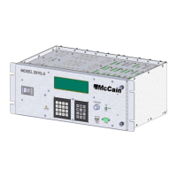
2070LX Controller – User Manual 37
Version 1.0
Jumper at ON position (pin-1 to pin-2): The processor outputs a state change on OUTPUT 39
(Monitor Watchdog Timer Input) every 100ms for 10 seconds or due to Set Output Command.
The watchdog output is sent to the output port #5 bit 8 and located at C1S connector pin-103.
Jumper at OFF position (pin-2 to pin-3): Causes no watchdog output. This feature is required to
operate with the Model 210 Monitor Unit.
Supervisory circuit
The supervisory circuit monitors the power supply of the processor and it asserts a reset if the power
supply drops below the threshold level of 4.63 VDC. The reset is an active low output that remains low by
140ms once power supply reaches the threshold level.
NRESET
This signal is the result of OR’ing the POWERUP and CPURESET signals at the isolation stage.
POWERUP is a signal from the Power Supply and is generated according to the conditions of the AC
input power; it is asserted if a power failure lasts more that 525ms ±25ms.
CPURESET is a signal coming from the CPU and it is a software reset.
They are received through the A3 slot, inverted, OR’ed and isolated. The NRESET signal enables a
buffer gate to generate the /RESETH signal that asserts the reset pin at processor.
BDM port
There is a 10-positions connector header (BDM) on the main board and it is used as a manufacturer-
specific BDM interface port for in-circuit programming and test on-board devices.
Parallel I/O ports
The parallel I/O ports consist of 64 input and 64 outputs that are present at the front connectors C1S and
C11S, see CONNECTOR’s PIN OUT section to see physical correspondence.
The front connectors are located on the connector board which is plugged to the main board through a
150-positions receptacle connector, so that the 64 inputs and 64 outputs reach the main board and are
routed to their corresponding circuits.
Parallel inputs ports
64 inputs using ground-true logic are provided; each input has an internal 10KOhm pull-up resistor to the
ISO +12VDC and a resistive network in order to adequate the signal so that the input is a logic "1" when
the input voltage at its field connector input is less than 3.5VDC, and is logic "0" when the input voltage
exceeds 8.5VDC.
The 64 inputs are distributed on eight octal buffers / line drivers; in order to send these inputs to the
processor they are arranged into four 16-bit groups called input banks.