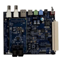
The ZLR964222L is a two-channel FXS line module designed to interface with the Microsemi Telephony Applications Platform (ZTAP) for evaluating the Le9642 miSLIC™ Subscriber Line Interface Device. This user guide provides sample operating instructions, schematics, bill of materials, and layout references. The ZLR964222L line module is designed to demonstrate a compact 2 FXS shared battery solution based on the new miSLIC Series. It features one Le9642 miSLIC Subscriber Line Interface Device (48-pin QFN) with a shared buck-boost ABS switching regulator.
Function Description:
The ZLR964222L line module provides two FXS ports suitable for worldwide operation. It supports a population option to convert to Le9641 1 FXS. The design is optimized for lowest cost on a 2 layer PCB on Microsemi’s SM2 board profile. It offers two channel cadenced ringing up to 85-Vpk and 5 REN ringer loads. Over-voltage / over-current protection for intra-building requirements is included. The module features an on-board 12 V input shared buck-boost ABS (BBABS) switching regulator circuit, designed for up to 600 Ω total loop. ZSI interface operation is supported up to 8.192 MHz (with ZTAP). DC sensing is outside the protection to allow support for VeriVoice foreign voltage tests. The compact 2 layer single sided component design and layout example measures 8.25cm² per FXS channel. On board Module ID ROM (MID) provides the default device profile, AC profile, DC profile, and ringing profile. A profile is defined by the Profile Wizard software tool for configuring Microsemi voice products. ZTAP and Microsemi Voice Toolkit (MiToolkit) with VP-API-II provides fully functional operation for complete two-channel FXS operation for extensive tests meeting the data sheet specifications.
Important Technical Specifications:
- Part Number: ZLR964222L
- Document ID#: PD-000196666
- Revision Number: 2.0
- Issue Date: November 2018
- Device: Le9642 miSLIC™ Subscriber Line Interface Device (48-pin QFN)
- FXS Ports: Two channels
- Ringing: Up to 85-Vpk, 5 REN ringer loads
- Loop Resistance: Up to 600 Ω
- ZSI Interface: Up to 8.192 MHz
- PCB Layers: 2 layers
- Component Design: Single sided
- Dimensions: 8.25 cm² per FXS channel
- Power Supply: On-board 12 V input shared buck-boost ABS (BBABS) switching regulator
- Capacitor, CSW1: 220uF 25V low impedance electrolytic (can be reduced to 10uF 25V X5R ceramic if additional bulk capacitance is present).
- Capacitor, CREF1: 10uF 6.3V X5R/X7R, minimum 0603 package size.
- PNP Power Transistor: 100V PNP, low Vce sat, Diodes/Zetex ZXTP2013 or equivalent. Collector (Vce) Voltage Rating: Vce=100V for up to 85Vpk ringing. Suitable Packages: SOT-223, SOT89. 100V Sources: ZXTP2013/ZX5T953/FZT953, CZT953. 140V Sources: ZXTP2014/ZX5T955/FZT955, CZT955. Thermal pad of at least 1cm².
- Inductors: 47uH, saturation current rating of 1.5A and greater. Inductance should not be degraded more than 30% at rated current.
- Switching Diodes: DSW1 (VBATL rectifier), DSW3 and DSW4 (BAV70 dual parallel diodes). Reverse voltage rating > 70V. Repetitive peak current rating > 600mA for a pair. Can be replaced with a single BAV23S.
- Power Consumption (CoC Profile):
- Shutdown: 5 mW (device), 5 mW (system)
- Disconnect: 21 mW (device), 22 mW (system)
- Low Power Idle: 39 mW (device), 43.4 mW (system)
- Idle/Standby: 89 mW (device), 107 mW (system)
- Active OHT: 173 mW (device), 223 mW (system)
- Active (normal or reverse polarity): 517 mW (device), 795 mW (system)
- Ringing (C1, C2, Other Channel LPI): 380-1442 mW (device), 1143-3426 mW (system)
- Power Consumption (Default Profile):
- Shutdown: 5 mW (device), 5 mW (system)
- Disconnect: 22 mW (device), 25 mW (system)
- Low Power Idle: 41.7 mW (device), 44.1 mW (system)
- Idle/Standby: 96.3 mW (device), 120.3 mW (system)
- Active OHT: 186.7 mW (device), 244.3 mW (system)
- Active (normal or reverse polarity): 580-1043 mW (device), 1018-1881 mW (system)
- Ringing (C1, C2, Other Channel LPI): 1375-1870 mW (device), 3362-4518 mW (system)
- Shared Buck-Boost ABS Switching Regulator Performance:
- Input Range: 10 to 14 VDC
- Supply Efficiency: Typically 50% to 75%
- Maximum Output Voltage: -95 VDC, limited by output capacitor rating.
- Ringing Voltage: Up to 85 Vpk
- Ringing Drive: 5 REN maximum at 60 Vrms single line
- VBATL Output Regulation: 2.0 % with 12 VDC input and -30 VDC output load varied from 0 to 30 mA
- Output Accuracy: -4 VDC to +4 VDC from the fixed ringing voltage setting
- Operating Frequency: 24 kHz LPM, 128 kHz MPM and HPM states
- Thermal Performance:
- Le9642 device has a thermal ePAD which must be soldered to a large copper area for heat dissipation.
- ZLR964222L module is designed with a 2 layer PCB to demonstrate functionality in a cost optimized system.
- Recommended ePAD configuration uses 0.215"/5.4 mm square pad tied to a ground plane with an 7x7 array of 0.33 mm vias for good thermal performance.
Usage Features:
- Quick Start:
- Assemble the components as shown in Figure 1 and connect a USB cable between the ZTAP’s USB port (J7101) and a PC.
- Plug the supplied 12V AC/DC adapter into the ZTAP’s +12 V input jack J6101.
- Apply power to the ZTAP and installed line module by switching SW6101 to the left. The system will boot up within about 20 seconds, initialize the installed line module, and automatically run the call control application. This allows pulse- and DTMF-dialed calls to be made between the telephony ports even without a PC attached.
- Start the MiToolkit application.
- When MiToolkit starts up, it will display a list of applications. Run the Mini-PBX application.
- When Mini-PBX starts, it will prompt for which serial port to use. If VP-Script is already running, Mini-PBX will know what port is being used. Note that the ZTAP Support Package software installation includes a Virtual COM Port Driver to support USB-to-serial UART interface on the ZTAP board.
- When Mini-PBX starts, it will identify the module plugged on the ZTAP and initialize it to the appropriate Idle state. The extension number, line type, and line state will also be displayed.
- Refer to the Microsemi Telephony Applications Platform User’s Guide for additional installation and operation details.
- Mini-PBX Configuration:
- The ZLR964222L line module is equipped with two FXS ports. Mini-PBX assigns extension numbers to each port, typically 100 and 101.
- To make an FXS to FXS call, connect two telephone sets to the two FXS ports on the line module.
- Mini-PBX detects off-hook, provides dial tone, and shows which extension is off-hook.
- To call the second FXS port (e.g., extension 101 from 100), dial 7101 (7 followed by extension number 101).
- Mini-PBX routes the call and initiates cadenced ringing (default defined in the MID).
- An audible ringback tone is provided to the calling extension.
- Caller ID information is generated to the called extension.
- Off-hook on the called extension triggers ring trip and sets up a voice path.
- Mini-PBX reflects the current line state for all lines.
- Profile Management:
- Profiles contain data strings for configuring functional blocks (Device, AC FXS, DC, Ringing, Tone, Ringing Cadence, Tone Cadence, Caller ID, Metering).
- Microsemi provides profiles for most countries and telephony standards.
- The Profile Wizard tool generates profiles.
- Default profiles are provided on the MID, but users can create new ones or edit existing profiles.
- Files for Device, AC, DC, and Ringing Profiles are available for use with the VP-API-II Lite software.
- A Software License Agreement (SLA) for the VP-API-II software is required for full VP-API-II license.
- Files for Device, AC, DC, Ringing, Tone, Cadence, and Caller ID for over 44 countries are available.
- The Profile Wizard Main Menu (Figure 7) allows selecting and generating profiles.
- The Ringing Profile Configuration Example (Figure 8) shows how to edit ringing parameters.
- Running new profiles involves starting MiToolkit, running Mini-PBX, and loading the new profile file.
- Adaptive Ringing:
- The ZLR964222L design includes an adaptive ringing feature to allow the device to adapt to heavier ringing loads in order to limit maximum input power.
- The ZLR964222L is designed to ring a maximum of 5REN at 60Vrms, but this does adaptive ringing feature can be enabled if the current that a heavy REN load is applied to a ringing power can be reduced to a lower level to support the heavier load.
- The ZTAP CLI command enables the feature on both channels, sets the power threshold to 1.2W per channel (26 * 39mW / 2) and sets the minimum ringing voltage to 83 % of the nominal ringing voltage.
- Adaptive ringing can be disabled using the ZTAP CLI command.
Maintenance Features:
- Thermal Management: The Le9642 device has a thermal ePAD that must be soldered to a large copper area for heat dissipation. For best thermal performance, a four layer PCB is recommended. Even with multi-layer boards it is recommended that multiple copper pours be used for thermal relief. The ZLR964222L module is designed with a 2 layer PCB to demonstrate functionality in a cost optimized system. In this case it is highly recommended that all components be placed on the top side of the PCB. The bottom side should be a solid ground plane with minimal voids that would disrupt heat dissipation.
- Over-temperature Protection: The Le9642 has a recommended maximum operating junction temperature of 145°C. The device will indicate a thermal fault at a junction temperature of 165°C. Depending on the setting of the VP_DEVICE_OPTION_ID_CRITICAL_FLT function in the VP-API-II, the device may either go to the Disconnect state or temporarily shut down the tip and ring drivers and turn them back on when the die temp is reduced. Note that the device will immediately cycle in and out of the temporary shutdown condition if a high power dissipation condition is present.
- xDSL Compatibility: Switching power supplies are inherently noisy. The buck-boost switching regulator is no exception. The collector node of the PNP will have high dv/dt signals with a voltage swing of 50 V or more at a frequency of up to 128kHz. Placing the switcher in close proximity of a DSL AFE can and most likely will cause degraded performance of the DSL interface. It is therefore extremely important that the PNP, inductor, and associated circuitry be placed at least one inch (2.5 cm) away from any DSL AFE signals.
- EMI/EMC Performance: Recommendations for EMI/EMC performance are proper supply decoupling/filtering and good digital design techniques. DVDD pins should have 0.01 µF decoupling caps and AVDD pins should have 0.1 µF decoupling caps for each supply pin of the device. An additional bulk decoupling cap such as a 1 µF ceramic or tantalum near the device is also recommended. There is also a filter between DVDD and AVDD that is required. A 1ohm resistor is placed between DVDD and AVDD and a 4.7uF ceramic cap is connected from AVDD to ground. The value of the resistor should not be increased or AVDD voltage may become degraded and out of spec.
- ZSI Interface: The ZSI interface is encouraged for 2 layer designs, as this reduces the number of signals that need to be routed. When using the ZSI interface, it is not necessary to place pull up or pull down resistors on the unused MPI interface pins. If resistors are used, they should be placed away from the device to prevent crowding around the device. If the resistors are placed next to the pins, this forces the ground layer on the bottom side to be significantly cut up.
- PNP Transistor Collector Tab: Under some operating conditions the thermal stress on the PNP power transistor (Q1) can be quite high. The collector tab of the PNP transistor should have a minimum PCB pad of 1cm x 1cm. More copper is better, but noise influence must also be considered. The collector node should never be placed close to the SWIS current sense net. Noise from the PNP collector can couple into the SWIS net and disrupt the stability of the power supply.
- Multilayer Design: Although this design is shown as a two-layer design, best performance can be achieved with a multilayer design that incorporates ground planes.