ZLR964222L Line Module User Guide
12
Microsemi Corporation Confidential and Proprietary
4.0 Circuit Design
4.1 Overview
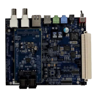
The ZLR964222L Line Module consists of a Le9642 miSLIC
TM
Subscriber Line Interface Device, line interface
circuit, one shared buck-boost ABS switching regulator circuit, and a host interface circuit for communication with
the Microsemi ZTAP platform. This chapter highlights some of the design considerations including component
selection and options.
The ZLR964222L line module design also allows easy conversion to a single channel Le9641 single channel
miSLIC device. The single channel option uses a fixed tracking buck-boost supply. The single buck-boost supply is
also just a population change to the BBABS power supply. This option demonstrates a single layout that can either
support 2 FXS or 1 FXS.
4.2 Le9642 Device
The Le9642 is a member of the miSLIC family of FXS devices from Microsemi designed for worldwide markets. The
Le9642 provides complete BORSCHT functions for two telephone line FXS ports. It features enhanced
functionality, lower BOM cost, and greater power efficiency while maintaining software compatibility with the VE880
Series. Device-level enhancements include the following:
• Low Power Idle Mode (LPIM) with < 51 mW/ch typical power consumption when
FXS_LOW_PWR termination type is used.
• Added ZSI Mode support for a smaller number of interface signals and less expensive isolation
(if required). This mode is supported by most leading residential gateway SoCs.
• New Supervision ADC for advanced testing, improved calibration and adaptive power
management.
The VP-API-II takes advantage of these and other enhancements in the Le9642 and offers greater programmability
and more efficient operation.
Please refer to the Le9642 miSLIC Subscriber Line Interface Device Data Sheet for more details about this device.
“ZLR964222L Line Interface Circuit” on page 13 shows the Le9642 and associated components. The designer
should note the following changes from previous VE880-based designs:
• Le9642 does not have separate ground pins. All ground is routed through the metal ePAD,
which is also used for thermal heat dissipation
•RREF
1
should be a precision 0.5% 25ppm resistor (75.0 K) in order to meet the data sheet
specifications. A 1% resistor may be used, but some device parameters may not meet the data
sheet specifications. Some parameters that would be affected are VBAT, VOC, ILA,VeriVoice
Accuracy etc.
4.3 ZSI Digital Interface
The ZSI digital interface is a synchronous full-duplex 4-wire communication link between the Le9642 device and the
host. The ZSI protocol multiplexes telephony audio, control and status information into the ZSI data stream. The
ZSI bus consists of 4 signals ZCLK, ZSYNC, ZMISO, and ZMOSI. The ZSI makes it possible to reduce the
number of pins on communication SoCs and VoIP processors and reduce the number of digital isolators for
applications such as DSL signal reinjection. Most common gateway SoCs support the ZSI interface. Refer to the
Le9642 Data Sheet for ZSI interface timing.
In order to perform half channel measurements or to debug or monitor the ZSI interface, the ZSI data stream can be
demultiplexed using a Microsemi ZSI Snooper board, Le71HP0418G. A footprint for header J1 is provided on the
ZLR964222L Line Module in order to interface to the Snooper board. To utilize this function, remove the four header