ZLR964222L Line Module User Guide
13
Microsemi Corporation Confidential and Proprietary
shunt resistors (RZSI1- RZSI4) and populate J1, Samtec FTSH-105-01-L-DV. This allows for cabling between the
ZLR964222L Line Module and the ZSI Snooper board to manipulate the ZSI data stream.
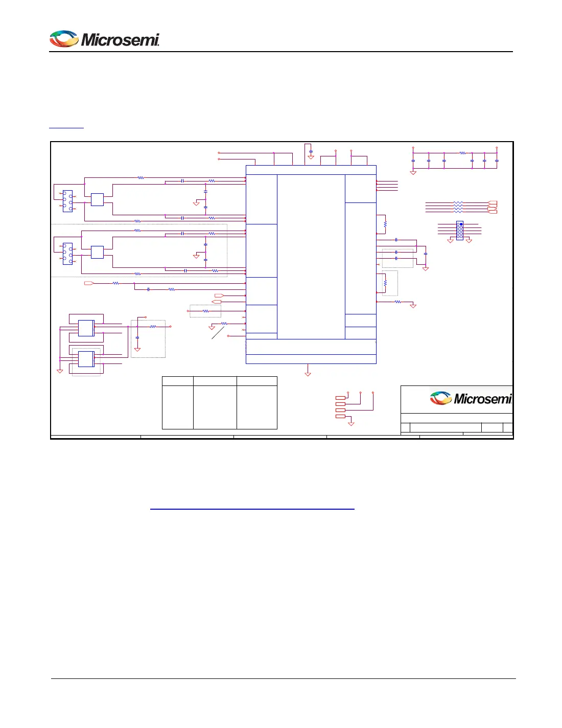
4.4 Line Interface Circuit
Figure 3 below shows the ZLR964222L simplified line interface circuit. Optional components and those used for
testing have been omitted. The complete circuit is shown in Section 7.
Figure 3 - ZLR964222L Line Interface Circuit
4.4.1 Surge Protection
The ZLR964222L line module design has series current limiting and shunt voltage limiting for lightning and surge
protection as shown in “ZLR964222L Line Interface Circuit” on page 13. This protection design uses Positive
Temperature Coefficient (PTC) thermistor devices to limit surge current. The purpose of the PTC is to provide
overcurrent protection during a power cross event. During a typical transient surge (i.e. due to a lighting strike), the
PTC simply acts like a low-value resistor limiting the surge current to a manageable level. In the event of a power
cross, the PTC behaves like a fuse. Since a power cross is a long term event, the PTC will heat up and transition
from a low resistance to a high resistance. After the event has been cleared, the PTC will return to a low resistance
value once again, assuming the ratings of the PTC have not been exceeded.
Voltage limiting is provided by Bourns TISP61089B programmable overvoltage SLIC protector. This device
provides a voltage clamp that is triggered by voltages slightly more negative than VBH. This protection scheme
protects both the Tip and Ring leads of the surged channel, limiting the voltage applied to either the TIPD or RINGD
pins of the device. The use of battery tracking protection permits the use of a VBAT
i
supplies rail near the device
maximum rating. Two single devices are used instead of a dual device to allow a lower cost single channel
population option.
A B C D E
4
3
2
1
NOTES
- Exposed pad on the Le9642 must be connected
through via holes to both side of top and bottom layer copper
and connected to a GND plane.
Locate CVDx next to DVDD, and CVAx next to AVDD pins.
ALL GROUNDS ARE VIA THE EPAD
- Recommended EPAD should be a 216mil square pad
with a 7 x 7 array of 13mil/.33mil vias. Vias should be
connected to the ground plane with solid connections.
TDC1
TAC1
TIPD1
RINGD1
RAC1
RDC1
TDC2
TAC2
TIPD2
RINGD2
RAC2
RDC2
Population Options for 2 FXS BB ABS and 1FXS BB
2 FXS BB ABS 1 FXS TrackerReference
RVS2 DNP1Meg 1% 0805
Table 1
RT2
CHL2
47.5K 1% 0402 DNP
CLFC1
4.7uF X5R 6.3V DNP
4.7uF X5R 6.3V0.1uF 10V
0805
See Table 1
0603
RVP1 DNP 0ohm 0603
De-populate for 1 FXS
U3 TISP61089BD DNP
See Table 1
See Table 1
A 10K pulldown resistor
is required on SWISZ if
the Le9641 1ch option is required.
Pin 24 is the ZSIn on Le9641
VBATL_VBAT
AGND
VBATH
3.3V
SWOUTY
VBSENSE1
SWISY
ZCLK
ZMOSI
ZSYNC
ZMISO
AGND
VBATH3.3V
AGND
AGND
3.3V
AGND
AGND
3.3V
AGND
AGND
AGND
3.3V
VBATL_VBAT
VBATH
3.3VA
3.3VA
AGND
VBATH
AGND AGND
AGND
AGND
VBATL_VBAT
VBATH
VBATL_VBAT
Title
Size Document Number Rev
Date: Sheet
of
Designer
0LFURVHPL3URSULHWDU\'RFXPHQW
ZLR964222L B3
Le9642 2 FXS Shared Buck-Boost ABS
B
45Monday, April 30, 2018
JLR
0LFURVHPL
)UHLGULFK/Q
%OGJ6XLWH
$XVWLQ7;
Title
Size Document Number Rev
Date: Sheet
of
Designer
0LFURVHPL3URSULHWDU\'RFXPHQW
ZLR964222L B3
Le9642 2 FXS Shared Buck-Boost ABS
B
45Monday, April 30, 2018
JLR
0LFURVHPL
)UHLGULFK/Q
%OGJ6XLWH
$XVWLQ7;
Title
Size Document Number Rev
Date: Sheet
of
Designer
0LFURVHPL3URSULHWDU\'RFXPHQW
ZLR964222L B3
Le9642 2 FXS Shared Buck-Boost ABS
B
45Monday, April 30, 2018
JLR
0LFURVHPL
)UHLGULFK/Q
%OGJ6XLWH
$XVWLQ7;
RTDCA1 1Meg 1%
RZSI1 0 Ohm
PTC1
MF-SD013/250
1 2
3 4
RVS1 1Meg
1%
SK2
TA-250-6
2
4
1
3
5
6
CRAC1 0.022uF
100V
RT2
47.5K
1%
RZSI2 0 Ohm
RRDCA1 1Meg 1%
RRAC1 10K 1%
RT1
47.5K
1%
SK1
TA-250-6
2
4
1
3
5
6
RZSI3 0 Ohm
RVS2 1Meg
1%
PTC2
MF-SD013/250
1 2
3 4
CV2
4.7uF
6.3V
CVP1
0.1uF
100V
RZSI4 0 Ohm
RTDCA2 1Meg 1%
CREF1
10uF
6.3V
CVIO1
0.01uF
16V
RV1
1R0 5%
RVP1 0R
CVD12
0.1uF
16V
CVD1
0.01uF
16V
CTD2
.022uF
100V
RRDCA2 1Meg 1%
U3
TISP61089BD
K1a
1
G
2
NC
3
K2a
4
K2b
5
A2
6
A1
7
K1b
8
CRD2
.022uF
100V
CHL2 4.7uF 6.3V
ZSI
Interface
Channel 1
Channel 2
POWER
N/C Do
Not Route
GROUND
Analog
Settings
Switch
Control
Channel 1
Channel 2
Switch
Control
U1
Le9642
VBL1
48
RVSD1
39
RSN1
1
AVDD2
35
RTV1
3
IHL1
5
TAC1
6
RAC1
7
TDC1
8
RDC1
9
LFC1
10
IREF
33
VREF
4
SWVSY
11
SWISY
13
SWCMPY
12
SWOUTY
16
DVDD1
15
ZSYNC
18
ZMISO
19
ZCLK
21
DVDHPI
23
SWOUTZ
17
SWCMPZ
25
SWISZ
24
SWVSZ
26
VDDSW
14
LFC2
27
RDC2
28
TDC2
29
RAC2
30
TAC2
31
IHL2
32
RTV2
34
RSN2
36
DVDD1V2
22
RSVD2
42
RINGD2
41
RSVD3
44
RSVD4
47
TIPD2
40
VBL2
37
RINGD1
45
TIPD1
46
VBH
43
ePAD_GND
49
AVDD1
2
ZMOSI
20
RVSD0
38
CCMP1 2.2nF
16V
RRAC2 10K 1%
CVA1
0.1uF
16V
CTAC1 0.022uF
100V
J1
DNP
12
34
56
78
910
CTAC2 0.022uF
100V
CTD1
.022uF
100V
RTAC1 10K 1%
CLFC1 0.1uF 16V
RCMP1 1Meg 1%
RREF1 75K
0.5%
RTAC2 10K 1%
CHL1 4.7uF 6.3V
CVA2
0.1uF
16V
RZ1 10K 1%
CRD1
.022uF
100V
CRAC2 0.022uF
100V
U2
TISP61089BD
K1a
1
G
2
NC
3
K2a
4
K2b
5
A2
6
A1
7
K1b
8
CV1
4.7uF
6.3V
PRING1
ZCLKi
ZSYNCi
ZMISOi
ZMOSIi
PTIP1
PTIP2
PRING2
ZCLKi
ZMISOi
ZMOSIi
ZSYNCi
PCLK
FS
DXA
DRA
ZCLKi
ZMISOi
ZMOSIi
ZSYNCi
PCLK
FS
DXA
DRA
PRING2
PTIP2
PTIP1
PRING1