ZLR964222L Line Module User Guide
List of Figures
4
Microsemi Corporation Confidential and Proprietary
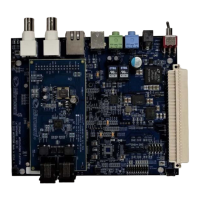
Figure 1 - ZTAP and ZLR964222L Line Module Setup . . . . . . . . . . . . . . . . . . . . . . . . . . . . . . . . . . . . . . . . . . . . . . 8
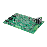
Figure 2 - ZLR964222L Line Module . . . . . . . . . . . . . . . . . . . . . . . . . . . . . . . . . . . . . . . . . . . . . . . . . . . . . . . . . . . . 9
Figure 3 - ZLR964222L Line Interface Circuit . . . . . . . . . . . . . . . . . . . . . . . . . . . . . . . . . . . . . . . . . . . . . . . . . . . . 13
Figure 4 - ZLR964222L Buck-Boost ABS Switching Regulator . . . . . . . . . . . . . . . . . . . . . . . . . . . . . . . . . . . . . . . 15
Figure 5 - Le9641 miSLIC Single Channel Population . . . . . . . . . . . . . . . . . . . . . . . . . . . . . . . . . . . . . . . . . . . . . 17
Figure 6 - Buck-Boost ABS to Fixed Tracking Buck-Boost Population . . . . . . . . . . . . . . . . . . . . . . . . . . . . . . . . . 18
Figure 7 - Profile Wizard Main Menu - ZLR964222L Project File. . . . . . . . . . . . . . . . . . . . . . . . . . . . . . . . . . . . . . 21
Figure 8 - Ringing Profile Configuration Example . . . . . . . . . . . . . . . . . . . . . . . . . . . . . . . . . . . . . . . . . . . . . . . . . 22
Figure 9 - Mini-PBX - Configuration Mode . . . . . . . . . . . . . . . . . . . . . . . . . . . . . . . . . . . . . . . . . . . . . . . . . . . . . . . 23
Figure 10 - Mini-PBX - Device Configuration . . . . . . . . . . . . . . . . . . . . . . . . . . . . . . . . . . . . . . . . . . . . . . . . . . . . . 23
Figure 11 - Two-Wire Return Loss (Narrowband) . . . . . . . . . . . . . . . . . . . . . . . . . . . . . . . . . . . . . . . . . . . . . . . . . 24
Figure 12 - Four-Wire Return Loss (Narrowband) . . . . . . . . . . . . . . . . . . . . . . . . . . . . . . . . . . . . . . . . . . . . . . . . . 25
Figure 13 - Receive Path (D to A) Attenuation Distortion (Narrowband) . . . . . . . . . . . . . . . . . . . . . . . . . . . . . . . . 26
Figure 14 - Transmit Path (A to D) Attenuation Distortion (Narrowband). . . . . . . . . . . . . . . . . . . . . . . . . . . . . . . . 26
Figure 15 - Receive Path (D to A) Gain Tracking (Narrowband) . . . . . . . . . . . . . . . . . . . . . . . . . . . . . . . . . . . . . . 27
Figure 16 - Transmit Path (A to D) Gain Tracking (Narrowband). . . . . . . . . . . . . . . . . . . . . . . . . . . . . . . . . . . . . . 27
Figure 17 - Receive Path (D to A) Total Distortion (Narrowband) . . . . . . . . . . . . . . . . . . . . . . . . . . . . . . . . . . . . . 28
Figure 18 - Transmit Path (A to D) Total Distortion (Narrowband) . . . . . . . . . . . . . . . . . . . . . . . . . . . . . . . . . . . . . 28
Figure 19 - Two-Wire Return Loss (Wideband) . . . . . . . . . . . . . . . . . . . . . . . . . . . . . . . . . . . . . . . . . . . . . . . . . . . 29
Figure 20 - Four-Wire Return Loss (Wideband). . . . . . . . . . . . . . . . . . . . . . . . . . . . . . . . . . . . . . . . . . . . . . . . . . . 29
Figure 21 - Receive Path (D to A) Attenuation Distortion (Wideband) . . . . . . . . . . . . . . . . . . . . . . . . . . . . . . . . . . 30
Figure 22 - Transmit Path (A to D) Attenuation Distortion (Wideband) . . . . . . . . . . . . . . . . . . . . . . . . . . . . . . . . . 30
Figure 23 - Receive Path (D to A) Gain Tracking (Wideband) . . . . . . . . . . . . . . . . . . . . . . . . . . . . . . . . . . . . . . . . 31
Figure 24 - Transmit Path (A to D) Gain Tracking (Wideband) . . . . . . . . . . . . . . . . . . . . . . . . . . . . . . . . . . . . . . . 31
Figure 25 - Receive Path (D to A) Total Distortion (Wideband) . . . . . . . . . . . . . . . . . . . . . . . . . . . . . . . . . . . . . . . 32
Figure 26 - Transmit Path (A to D) Total Distortion (Wideband). . . . . . . . . . . . . . . . . . . . . . . . . . . . . . . . . . . . . . . 32
Figure 27 - Adaptive Ringing Behaviour, 0 REN to 5REN . . . . . . . . . . . . . . . . . . . . . . . . . . . . . . . . . . . . . . . . . . . 36
Figure 28 - Top Etch and Silk Screen . . . . . . . . . . . . . . . . . . . . . . . . . . . . . . . . . . . . . . . . . . . . . . . . . . . . . . . . . . 45
Figure 29 - Bottom Etch and Silk Screen. . . . . . . . . . . . . . . . . . . . . . . . . . . . . . . . . . . . . . . . . . . . . . . . . . . . . . . . 45
Figure 30 - Microsemi 48 pin QFN PCB Footprint . . . . . . . . . . . . . . . . . . . . . . . . . . . . . . . . . . . . . . . . . . . . . . . . . 46