MDS 05-2415A01, Rev. A APPENDIX B B-3
When an RF carrier is detected, the receiver squelch forces DCD true and the receiver re-
ceives the FSK (Frequency Shift Keyed) signal just as it would any FM modulated signal.
The recovered audio is fed to the modem board which determines the peak excursion of the
received waveform in each direction. The center voltage (halfway) between these excursions
is used as a “slice” voltage for comparison with the incoming waveform. The output of the
comparator is square wave TTL data, identical to that transmitted by the remote station. This
is then fed to U31, the interface IC on the transceiver main board. Received data is then
delivered on the transceiver’s INTERFACE connector–Pin 3.
Synchronizing Data
For asynchronous operation, the modem synchronizes to the incoming transmit data. For
synchronous operation, the modem generates the transmit clock timing signal for use by
external equipment. Data changes on the rising edge of the TX clock signal, and the modem
samples the data on the falling edge of the clock signal.
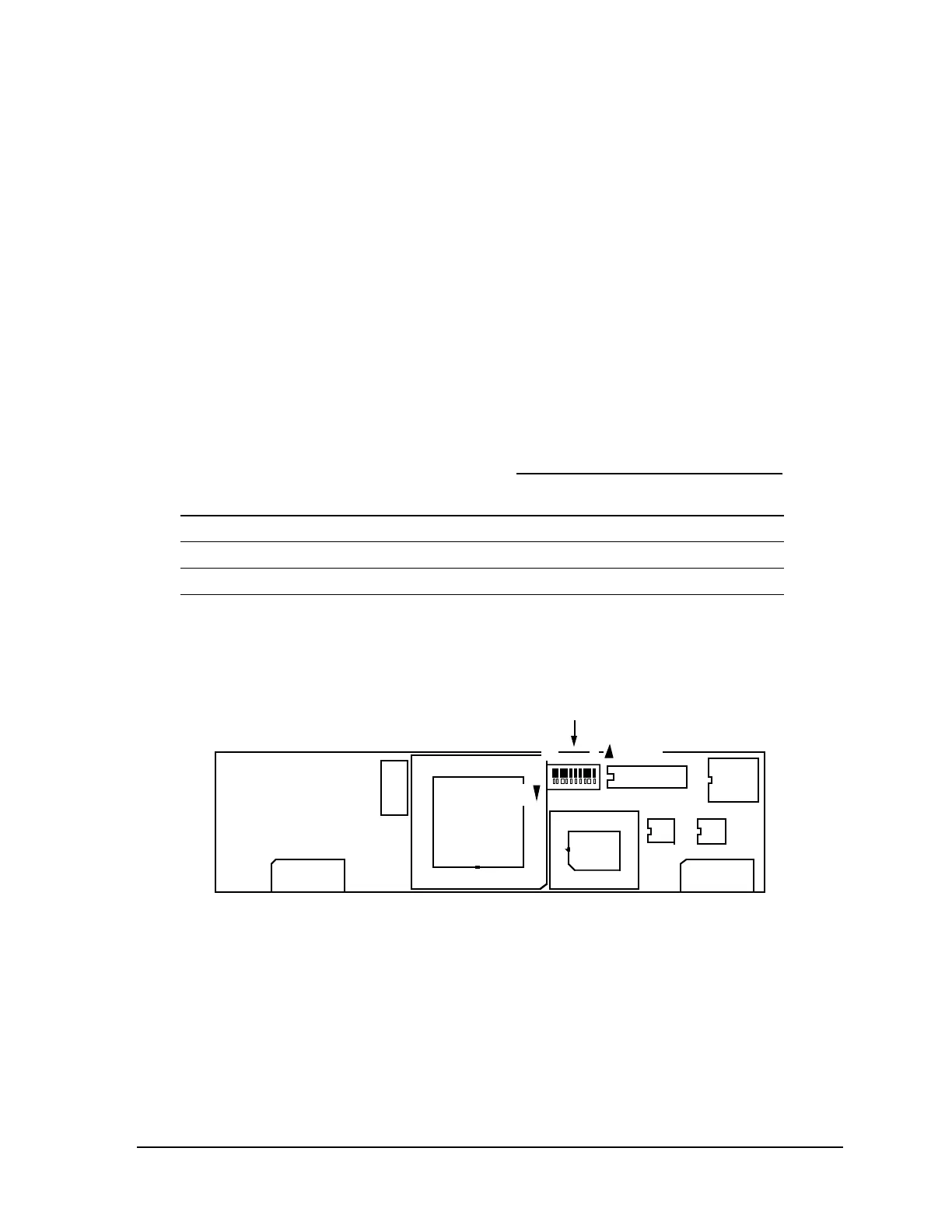
Table B-1. Settings for the MDS 4800 bps Modem’s Configuration Switch S1
MODEM SWITCHES
SYNCHRONIZATION
12345678
Synchronous w/internal clock O O O O O O O O
Synchronous w/external clock O C O O O O O O
Asynchronous—Preferred
(factory default setting)
OCOC OOOO
LEGEND: C = CLOSED = ON O = OPEN = OFF
P8 P6
S1
CONFIGURATION
8 1
U6
U5
OPEN
CLOSED
Figure B-2. MDS 4800 bps Modem Assembly Diagram,
P/N 03-1831A01