App-114
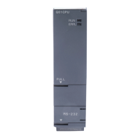
Appendix 1.5 Operation Processing Time of LCPU
The processing time for the individual instructions are shown in the table on the following pages.
Operation processing times can vary substantially depending on the nature of the sources and
destinations of the instructions, and the values contained in the following tables should therefore
be taken as a set of general guidelines to processing time rather than as being strictly accurate.
Appendix 1.5.1 Subset instruction processing time
The following describes the subset instruction processing time.
1. The subset instruction processing time table shown in (1) applies when the device
used in an instruction satisfies either of the conditions.
(See section 3.5.1 for the device conditions for subset instruction processing.)
2. When using the file register or a module access device (U3En\G10000 or higher),
add the processing time for each instruction, with reference to the adding time in (2).
3. When using an F,T(ST),C device with an OUT/SET/RST instruction, add the
processing time for each instruction, with reference to the adding time in (3).
4. Since the processing time of each instruction is not constant due to the cache
function in the LCPU, the minimum value and the maximum value are described.
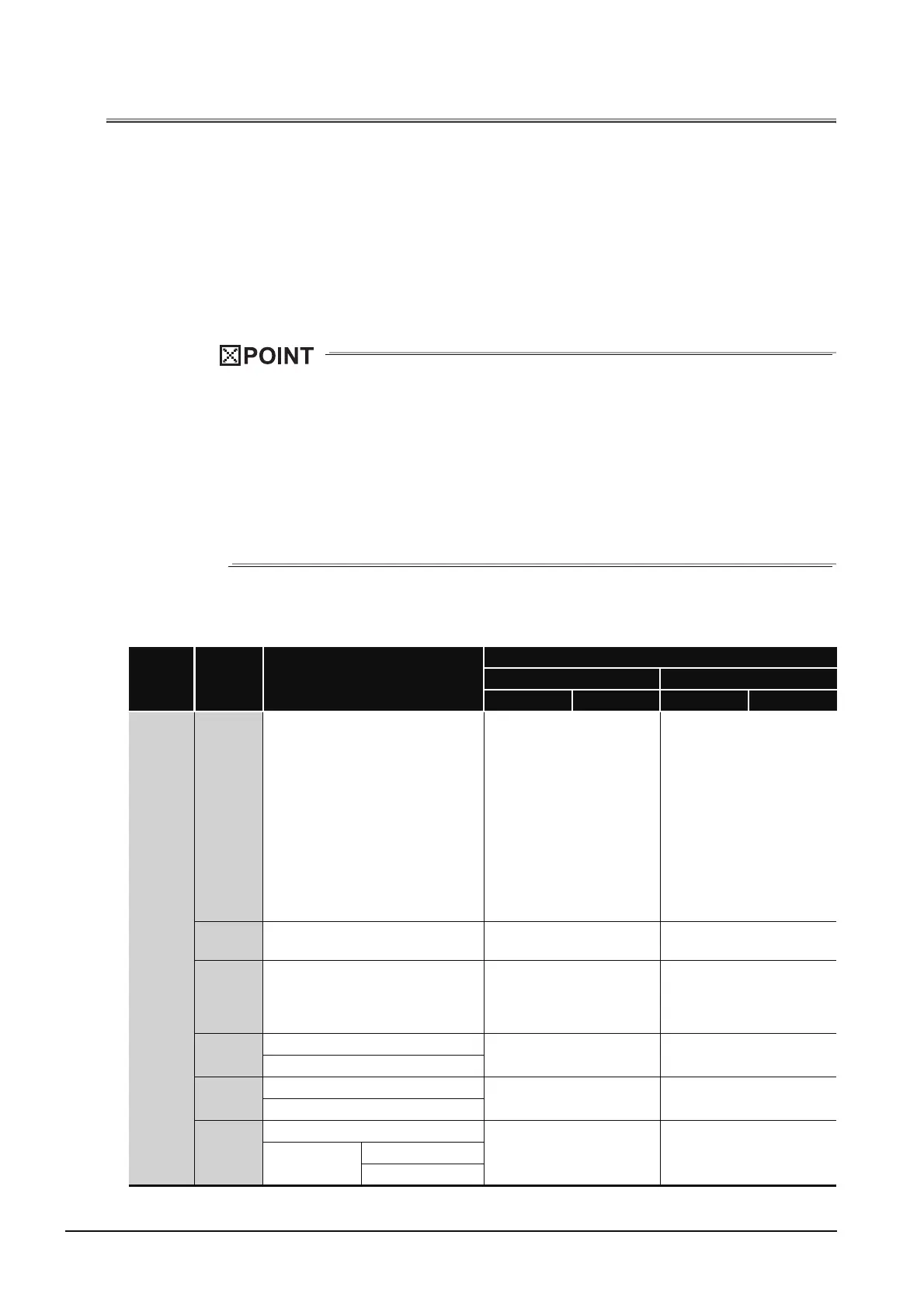
(1) Subset instruction processing time table
(a) When using L02CPU, L26CPU-BT.
Category Instruction Condition (Device)
Processing Time (µs)
L02CPU L26CPU-BT
Min. Max. Min. Max.
Sequence
instruction
LD
LDI
AND
ANI
OR
ORI
LDP
LDF
ANDP
ANDF
ORP
ORF
When executed 0.040 0.0095
LDPI
LDFI
When executed 0.120 0.0285
ANDPI
ANDFI
ORPI
ORFI
When executed 0.160 0.038
OUT
When not changed
0.040 0.0095
When changed
OUT H
When not changed
0.040
0.0095
When changed
SET
RST
When not executed
0.040 0.0095
When executed
When not changed
When changed
 Loading...