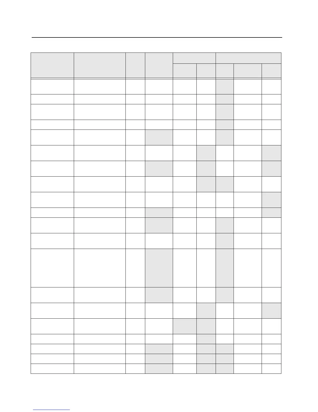
7-6 Troubleshooting Tables: List of Board and IC Signals
middle_side_butto
n
Middle side button
input
T20 0 Input None
Input Pull-
down
mako_intx Mako main interrupt P15 0 Input None
Input None
mako_usb_intx Mako USB interrupt AA9 0 Input None
Input Pull-
down
mako_option_intx Mako Option interrupt Y12 0 Input None
Input None
Unused and Unwired
OMAP Pin
M14
Input Pull-
down
Input Pull-
down
top_display_cs Top LCD SPI chip
select
P3 0 Output
1 Output
Unused and Unwired
OMAP Pin
V19 Output 0 Output
mako_cs Mako IC SPI chip
select
N15 1 Output Input Pull-
down
mortable Specifies Mobile or
Portable hardware
W13 0=Porta-
ble
Input None 0 Output
gcai_gpio3 GPIO3 AA15 Input None 0 Output
gcai_gpio4 GPIO4 R14 Input None Input Pull-
down
bluetooth_ptt PTT signal from Blue-
tooth AVR
Y5 0=Pressed Input Pullup
Input Pull-
down
f2_timer_input_ca
pture
"Receives one of
three timing signals
mux'ed through CPLD
- Abacus Sync,
DMCS, Ramp DAC
Trigger.
"P20
Input Pull-
down
Input Pull-
down
bt_avr_status AVR status read by
OMAP
P18
Input Pullup Input Pull-
down
enc_wakeup MACE encryption
wakeup
A6 1 Output
1 Output
enc_reset MACE encryption
reset
B6 0 I/O Pullup 1 I/O Pullup
5V_pwm_en Forces SW5 to PWM P14 1 Output
Pullup 0 Output Pullup
gcai_gpio2 GPIO2 C13
Input None Input None
gcai_gpio1 GPIO1 C11
Input None Input None
gcai_gpio0 GPIO0 M7
Input None Input None
Table 7-7. Overall GPIO pin functions (Continued)
Signal Name Description
Pin or
Ball #
Active State
SW Initialized HW Reset
Direction
*
PU State Direction
*
PU
or
PD
 Loading...