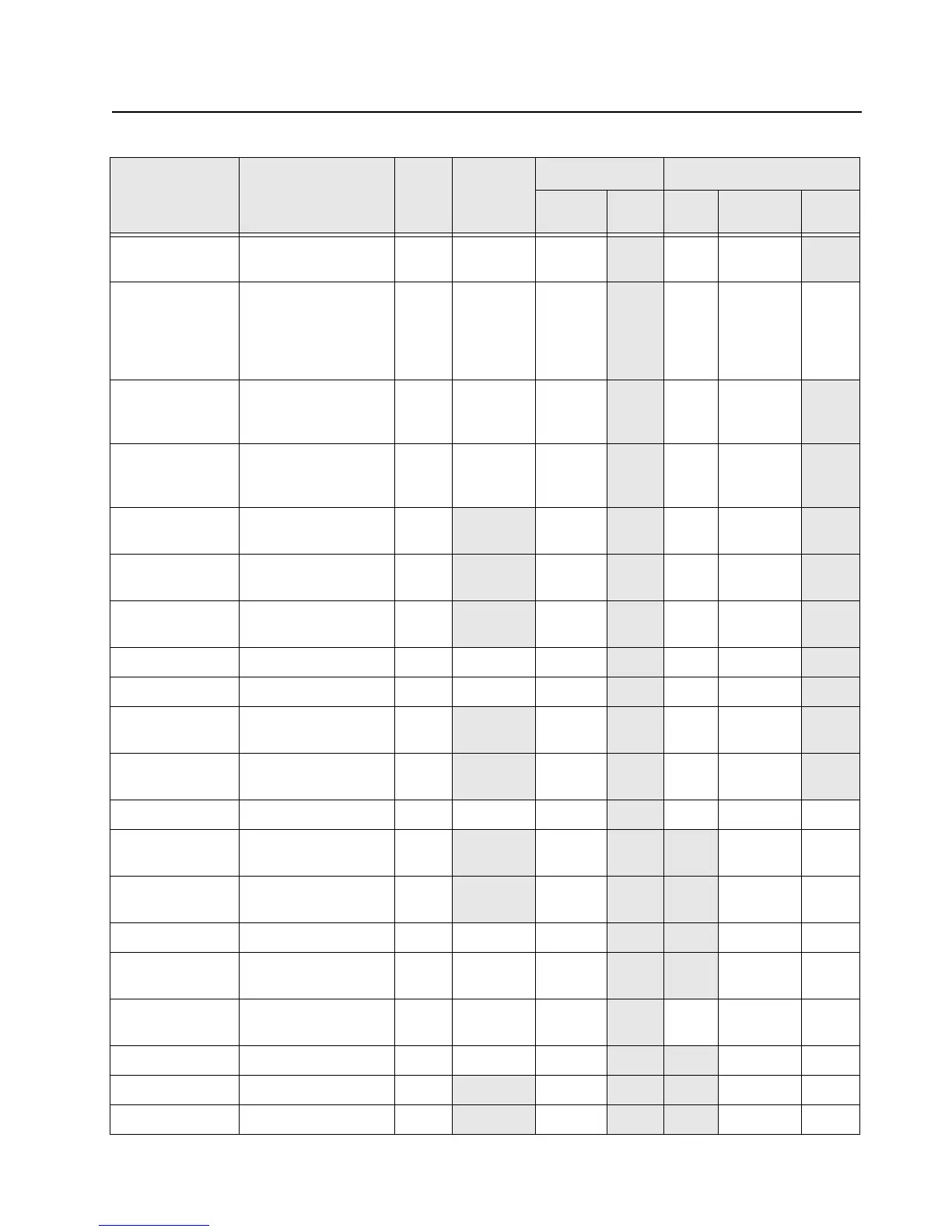
Troubleshooting Tables: List of Board and IC Signals 7-7
gcai_vbus_i_limit Current limit select for
GCAI VBUS
C6 1=500mA Output
0 Output
f2_paramp_mon Factory use to test F2
transmit timing. Allows
TX/RX signal to
appear on GCAI
GPIO3.
C5 1=Factory
Test
Output
Pullup 0 Output Pullup
top_disp_data_ctr
l
Select for data or con-
trol on top display(Not
Used in WWP)
P12 1=data Output 0 Output
top_display_reset Reset for color front
display( Not Used in
WWP)
M12 0 Output 1 Output
Unused and Unwired
OMAP Pin
N13 Output 0 Output
Unused and Unwired
OMAP Pin
M14 Output 0 Output
Unused and Unwired
OMAP Pin
N14 Output 0 Output
gps_shutdown Shutdown to GPS D12 0 Output 0 Output
rf_reset Reset to RF board A8 0 Output 0 Output
Unused and Unwired
OMAP Pin
B7 Output 0 Output
Unused and Unwired
OMAP Pin
B8 Output 1 Output
C7 0 Output None 1 Output None
Unused and Unwired
OMAP Pin
J2
Input None Input None
Unused and Unwired
OMAP Pin
M8
Input None Input None
bt_usb_boot Bluetooth 'boot' signal P8 0 Output
None Input None
bt_avr_reset Bluetooth AVR32
Reset signal
M13 0 Output
None Input
key_fail_switch Enables keyload path
for MACE secure.
A12 1 Output
0 Output
NC Not Used M6 TBD Input
Pullup Input None
NC Not Used N11
Input None Input 3
NC Not Used K14
Input None Input None
Table 7-7. Overall GPIO pin functions (Continued)
Signal Name Description
Pin or
Ball #
Active State
SW Initialized HW Reset
Direction
*
PU State Direction
*
PU
or
PD
 Loading...