UHF Band 2 (450–512/520 MHz) 25–40 W LDMOS Frequency Synthesis Section 13: 2-7
6881091C63-F
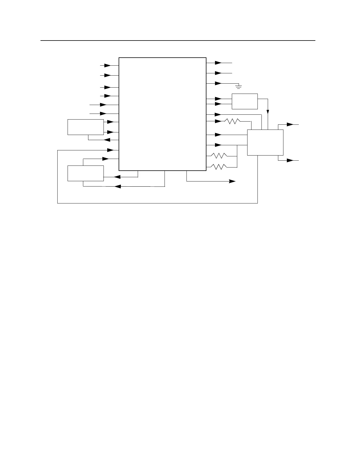
Figure 13-3 UHF Synthesizer Block Diagram
Output LOCK (U5201-4) provides information about the lock status of the synthesizer loop. A high
level at this output indicates a stable loop. IC U5201 provides the 16.8 MHz reference frequency at
pin 19.
The serial interface (SRL) is connected to the µP via data line DATA (U5201-7), clock line CLK
(U5201-8), and chip enable line CSX (U5201-9).
4.3 Voltage Controlled Oscillator (VCO)
The voltage controlled oscillator (VCO), shown in Figure 13-4, consists of a VCO buffer IC
(VCOBIC, U5301), TX and RX tank circuits, external RX buffer stages, and modulation circuits.
The VCOBIC together with Fractional-N synthesizer (U5201) generates the required frequencies in
both transmit and receive modes. The TRB line (U5301, pin 19) determines which tank circuits and
internal buffers are to be enabled. A high level on TRB enables TX tank and TX output (pin 10), and
a low enables RX tank and RX output (pin 8). A sample of the signal from the enabled output is
routed from U5301, pin 12 (PRESC_OUT), via a low-pass filter of U5201, pin 32 (PREIN).
A steering line voltage (VCTRL) between 3.0 V and 10.0 V at varactor diode CR5311 tunes the full
TX frequency range (TXINJ) from 450 MHz to 512 (or 520) MHz, and at varactor diodes CR5301,
CR5302, and CR5303 tunes the full RX frequency range (RXINJ) from 405 MHz to 467 MHz. The
tank circuits uses the Hartley configuration for wider bandwidth. For the RX tank circuit, external
transistor Q5301 is used in conjunction with the internal transistor for better side-band noise.
DATA
CLK
CEX
MODIN
VCC, DC5 V
XTAL1
XTAL2
WARP
PREIN
VCP
REFERENCE
OSCILLATOR
VOLTAGE
MULTIPLIER
DATA (U0101 PIN 100)
CLOCK (U0101 PIN 1)
CSX (U0101 PIN 2)
MOD IN (U0221 PIN 40)
+5 V (U4211 PIN 1)
7
8
9
10
13, 30
23
24
25
32
47
VMULT2 VMULT1
BIAS1
SFOUT
AUX3
AUX4
IADAPT
IOUT
GND
FREFOUT
LOCK
4
19
6, 22, 33, 44
43
45
3
2
28
14
15
40
FILTERED 5V
STEERING
LOCK (U0101 PIN 56)
PRESCALER IN
FREF (U0221 PIN 34)
39
BIAS2
41
48
5, 20, 34, 36
+5 V (U4211 PIN 1)
AUX1
VDD, DC5 V
MODOUT
U5201
LOW VOLTAGE
FRACTIONAL-N
SYNTHESIZER
AUX2
1 (NU)
BWSELECT
VCO Bias
TRB
To IF
Section
TX RF INJECTION
(1ST STAGE OF PA)
LO RF INJECTION
VOLTAGE
CONTROLLED
OSCILLATOR
LINE
2-POLE
LOOP
FILTER
 Loading...