8-5
3) Video Bias Circuit
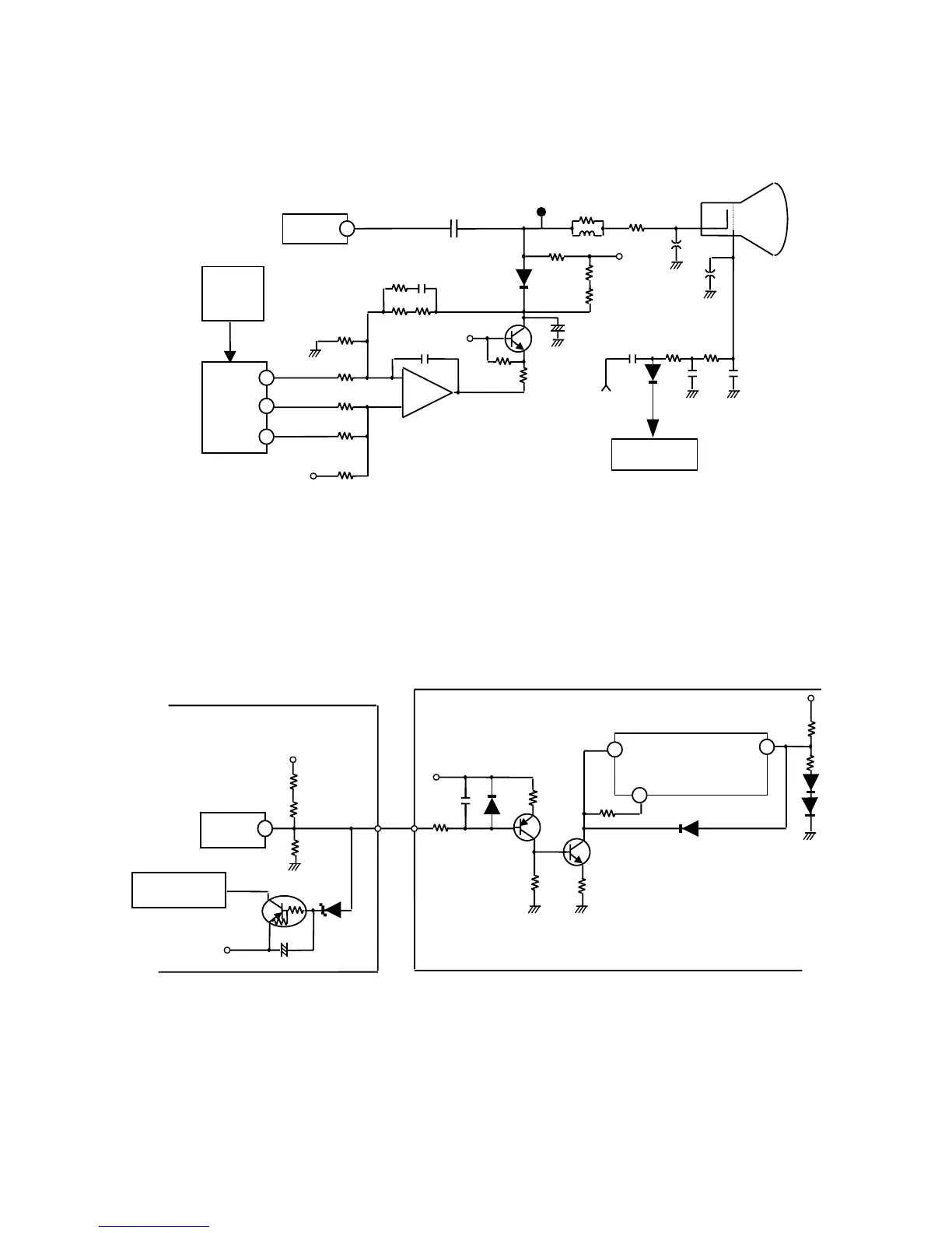
The video signal is amplified maximum 45Vpp in IC721 output, then the signal is done DC bias by video
bias circuit through C729G. This DC voltage varies when cut off adjustment and brightness adjustment.
The video bias circuit consists of fixed voltage circuit construction with op-amp. Q741G is used high-
voltage transistor due to get approx.80V to 170V at cathode black level voltage.
SUB BIAS, G BIAS and G BRT which are output from DAC IC751 are mixed at the op-amp IC742.
(Fig 1.3) Brightness and Cut-off Control
4) ABL Circuit
The ABL circuit consists of the part (Q771,Q772 and peripherals) which detects and amplifies the current
flowing to the CRT anode, and the other parts (IC711) which control the gain of the video signal (R,G and B).
The ABL circuit limits the amplitude of the video signal and serves to keep the maximum average current
flowing to the CRT up to 750μA. When the anode current is less than 750μA, Q772 does not operate. And
the anode current attempts to exceed 750μA, Q772 operates and the voltage of IC711 pin 15 drops, the
gain of IC711 drops. After saturation of IC711 pin 15, D713 becomes ON, then IC711 pin 30 drops. This is
the voltage that decides the black level of IC711 video output. Therefore back raster becomes dark.
(Fig 1.4) ABL Circuit
Cathod
R74GG
IC801
CPU
C729G
R742G
D741G
I
2
C BUS
-
+
+12V
C744G
R747G
R748G
Q741G
R749G
Auto Adjust
Blanking Circuit
R74AG
R744G R743G
R746G
+