https://reference.digilentinc.com/reference/programmable-logic/nexys-a7/reference-manual 18/30
(https://reference.digilentinc.com/_detail/reference/programmable-
logic/nexys-a7/n4o.png?id=reference%3Aprogrammable-logic%3Anexys-
a7%3Areference-manual)
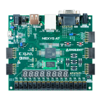
Figure 8.1.2 VGA Horizontal Synchronization
pixel of information. The VS signal defines the “refresh” frequency
of the display, or the frequency at which all information on the
display is redrawn. The minimum refresh frequency is a function of
the display’s phosphor and electron beam intensity, with practical
refresh frequencies falling in the 50Hz to 120Hz range. The
number of lines to be displayed at a given refresh frequency defines
the horizontal “retrace” frequency. For a 640-pixel by 480-row
display using a 25 MHz () pixel clock and 60 +/-1Hz refresh, the
signal timings shown in Figure 8.1.3 can be derived. Timings for
sync pulse width and front and back porch intervals (porch
intervals are the pre- and post-sync pulse times during which
information cannot be displayed) are based on observations taken
from actual VGA displays.
(https://reference.digilentinc.com/_detail/reference/programmable-logic/nexys-a7/n4p.png?id=reference%3Aprogrammable-logic%3Anexys-
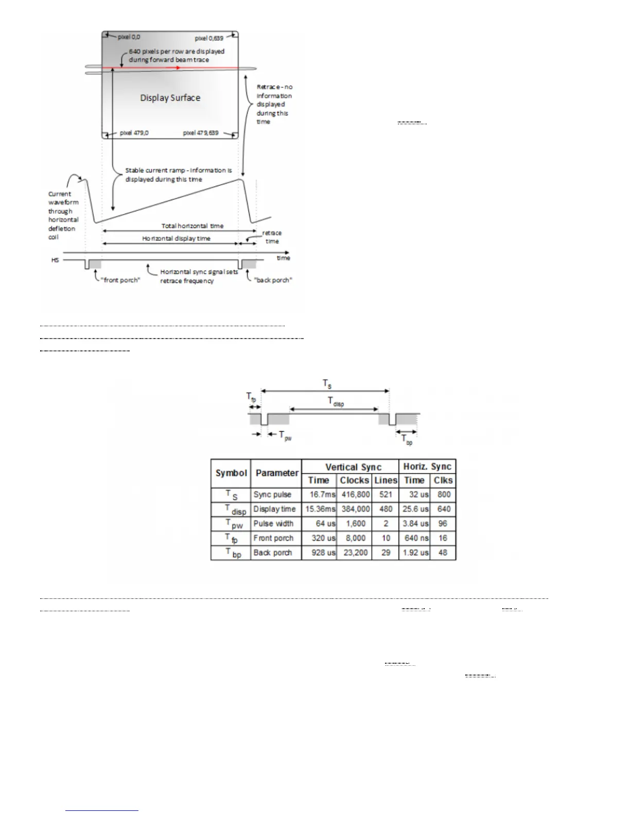
a7%3Areference-manual) Figure 8.1.3 Signal Timings for a 640-Pixel by 480-Row Display Using a 25 MHz () Pixel Clock and 60 Hz () Vertical Refresh
A VGA controller circuit, such as the one diagrammed in Figure 8.1.4, decodes the output of a horizontal-sync counter driven by the pixel
clock to generate HS signal timings. You can use this counter to locate any pixel location on a given row. Likewise, the output of a vertical-
sync counter that increments with each HS pulse can be used to generate VS signal timings, and you can use this counter to locate any given
row. These two continually running counters can be used to form an address into video RAM (). No time relationship between the onset of
the HS pulse and the onset of the VS pulse is specified, so you can arrange the counters to easily form video RAM () addresses, or to
minimize decoding logic for sync pulse generation.