Platform Adaptation and Bring-Up
Jetson Nano Platform Adaptation and Bring-Up Guide DA_09361-002 | 17
Go Through the Schematics
Refer to the P3449 carrier board’s schematic file,
P3449_B01_Concept_schematics.pdf, which is in Jetson Nano Developer Kit Carrier
Board Design Files. Contact your NVIDIA representative for further information.
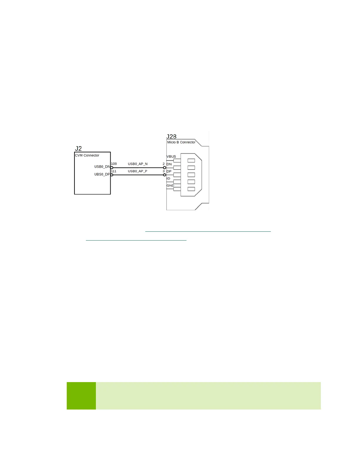
Check the USB connectors on the P3449 carrier board and find the wired socket location
to P3448.
• USB 2.0 signal pins D+/D− (DP and DN) wire out from J28 and lead to 111
(USB0_DP) and 109 (USB0_DN) on the CVM socket.
The USB 2.0 Micro B connector, J28, supports only HighSpeed mode, and does not have
USB 3.0 signal pairs. See the Tegra X1 (SoC) Technical Reference Manual
(TRM) and
consult Jetson Nano Product Design Guide for further information before you design
your custom board.
From the schematic, you can see that for J28:
• The USB 2.0 signal pair is wired to UTMI pad 0 (USB2 port 0).
The External Connector Class (extcon)
External connectors, which may have different types of cables attached (USB, TA,
HDMI, Analog A/V, and others), often have device drivers that detect state changes at
the port, and separate device drivers that do something according to the state changes.
The External Connector Class, extcon, supports the use of a notifier for passing
information such as state changes between device drivers.
Port switching between the roles of an OTG port is generally controlled by the host
driver (xHCI) and device driver (xUDC), and can be defined by the state of the ID pin
and the VBUS_DETECT pin.
Note:
Because its ID pin is floating, J28 is fixed in the device role in the Jetson Nano
Developer Kit. It cannot function as a host, e.g. to connect a flash drive,
keyboard, or mouse.

 Loading...


