Platform Adaptation and Bring-Up
Jetson Nano Platform Adaptation and Bring-Up Guide DA_09361-002 | 18
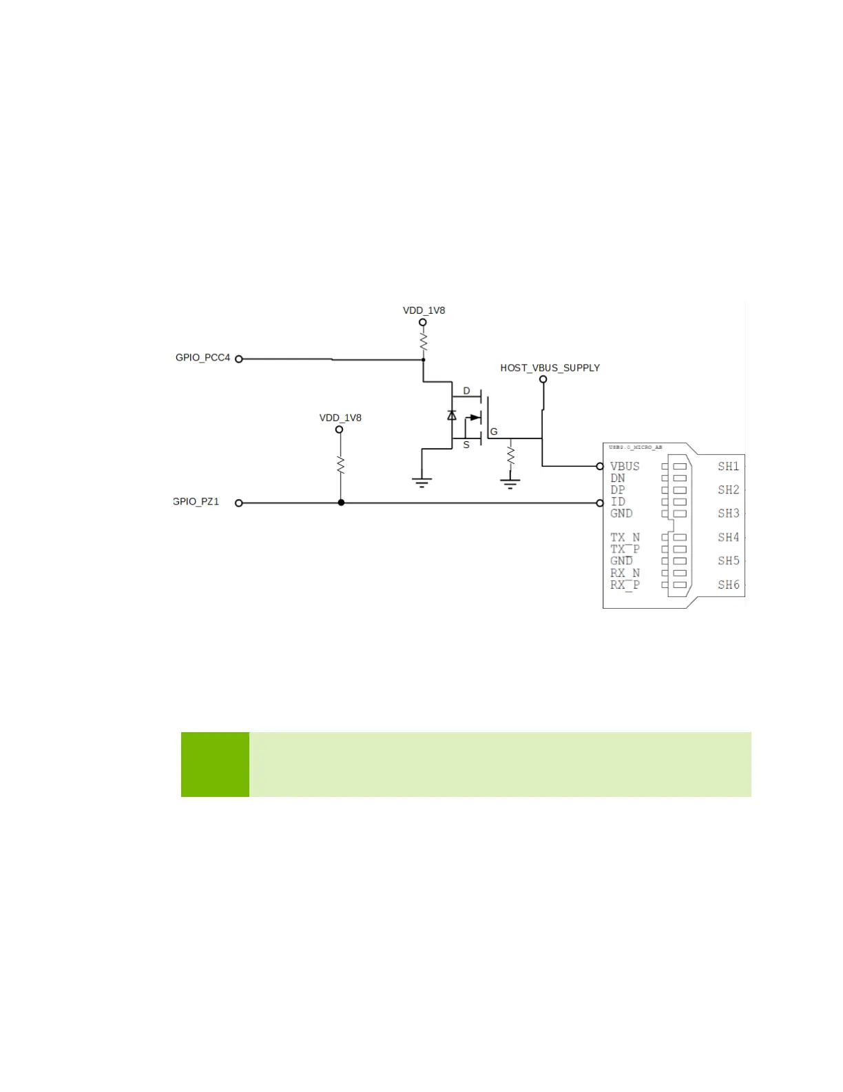
For example, suppose GPIO_PCC4 is the VBUS_DETECT pin and GPIO_PZ1 is the ID
pin. To complete the device tree node:
1. Find the corresponding GPIO states on the VBUS_DETECT pin and ID pin.
Generally, the ID pin is designed as internal pull high (logical high). With a Type A
plug connected the ID pin is pulled to ground (logical low), while with a Type B
plug connected or no cable connected it remains logical high.
The operation of the VBUS_DETECT pin depends on the device’s design. Consider
the schematic in Figure 2, for example:
Figure 2. Example of an OTG port's general design
With a Type B plug connected VBUS_DETECT is logical low because VBUS is
provided from an external power supply. When no cable is connected it is logical
high.
Note:
VBUS_DETECT is initially logical high, then logical low because VBUS is
provided by the host controller. Therefore the state of the VBUS_DETECT
pin does not matter when the OTG port is operating in the host role.
2. Create a table of GPIO states and their corresponding output cable states like the one
in Table 3.

 Loading...


