EasyManuals Logo
Home>Nvidia>Microcontrollers>JETSON TX2

Nvidia JETSON TX2 User Manual

Nvidia JETSON TX2
103 pages
To Next Page IconTo Next Page
To Previous Page IconTo Previous Page
Page #67 background imageLoading...
Page #67 background image
NVIDIA Jetson TX2/TX2i OEM Product Design Guide
JETSON TX2/TX2i OEM PRODUCT | DESIGN GUIDE | 20180618 67
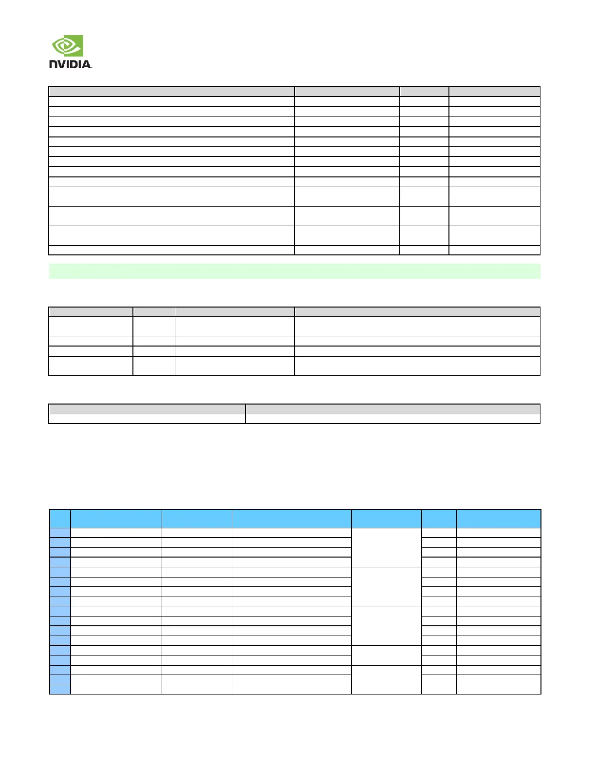
Table 72. SPI Interface Signal Routing Requirements
Parameter
Requirement
Units
Notes
Max Frequency
65
MHz
Configuration / Device Organization
3
load
Max Loading (total of all loads)
15
pF
Reference plane
GND
Breakout Region Impedance
Minimum width & spacing
Max PCB breakout delay
75
ps
Trace Impedance
50 60
±15%
Via proximity (Signal to reference)
< 3.8 (24)
mm (ps)
See Note 1
Trace spacing Microstrip / Stripline
4x / 3x
dielectric
Max Trace Length/Delay (PCB Main Trunk) Point-Point
For MOSI, MISO, SCK & CS 2x-Load Star/Daisy
195 (1228)
120 (756)
mm (ps)
Max Trace Length/Delay (Branch-A) 2x-Load Star/Daisy
for MOSI, MISO, SCK & CS
75 (472)
mm (ps)
Max Trace Length/Delay (Branch-B) 2x-Load Star/Daisy
for MOSI, MISO, SCK & CS
75 (472)
mm (ps)
Max Trace Length/Delay Skew from MOSI, MISO & CS to SCK
16 (100)
mm (ps)
At any point
Note:
Up to 4 signal Vias can share a single GND return Via
Table 73. SPI Signal Connections
Module Pin Names
Type
Termination
Description
SPI[2:0]_CLK
I/O
SPI0_CLK has 120
(on the module).
SPI Clock.: Connect to Peripheral CLK pin(s)
SPI[2:0]_MOSI
I/O
SPI Data Output: Connect to Slave Peripheral MOSI pin(s)
SPI[2:0]_MISO
I/O
SPI Data Input: Connect to Slave Peripheral MISO pin(s)
SPI2_CS[1:0]#
SPI[1:0]_CS0#
I/O
SPI Chip Selects.: Connect one CS_N pin per SPI IF to each Slave
Peripheral CS pin on the interface
Table 74. Recommended SPI observation (test) points for initial boards
Test Points Recommended
Location
One for each SPI signal line used
Near the module & Device pins.
12.3 UART
Jetson TX2/TX2i brings five UARTs out to the main connector. One of the UARTs is used for the WLAN/BT on Jetson TX2 or
as UART3 at the connector depending on the setting of a multiplexor. See Table 76 for typical assignments of the UARTs.
Table 75. UART Pin Descriptions
Pin #
Module Pin Name
Tegra Signal
Usage/Description
Usage on the Carrier
Board
Direction
Pin Type
H11
UART0_CTS#
UART1_CTS
UART 0 Clear to Send
Debug Header
Input
CMOS 1.8V
G11
UART0_RTS#
UART1_RTS
UART 0 Request to Send
Output
CMOS 1.8V
G12
UART0_RX
UART1_RX
UART 0 Receive
Input
CMOS 1.8V
H12
UART0_TX
UART1_TX
UART 0 Transmit
Output
CMOS 1.8V
E10
UART1_CTS#
UART3_CTS
UART 1 Clear to Send
Serial Port Header
Input
CMOS 1.8V
E9
UART1_RTS#
UART3_RTS
UART 1 Request to Send
Output
CMOS 1.8V
D10
UART1_RX
UART3_RX
UART 1 Receive
Input
CMOS 1.8V
D9
UART1_TX
UART3_TX
UART 1 Transmit
Output
CMOS 1.8V
A15
UART2_CTS#
UART2_CTS
UART 2 Clear to Send
M.2 Key E
Input
CMOS 1.8V
A16
UART2_RTS#
UART2_RTS
UART 2 Request to Send
Output
CMOS 1.8V
B15
UART2_RX
UART2_RX
UART 2 Receive
Input
CMOS 1.8V
B16
UART2_TX
UART2_TX
UART 2 Transmit
Output
CMOS 1.8V
G9
UART3_CTS#
UART4_CTS_N
UART 3 Clear to Send (muxed on TX2)
Not assigned
Input
CMOS 1.8V
G10
UART3_RTS#
UART4_RTS_N
UART 3 Request to Send (muxed on TX2)
Output
CMOS 1.8V
H9
UART3_RX
UART4_RX
UART 3 Receive (muxed on TX2)
Optional source of
UART on Exp. Header
Input
CMOS 1.8V
H10
UART3_TX
UART4_TX
UART 3 Transmit (muxed on TX2)
Output
CMOS 1.8V
D5
UART7_RX
UART7_RX
UART 7 Receive
Not Assigned
Input
CMOS 1.8V

Other manuals for Nvidia JETSON TX2

Questions and Answers:

Question and Answer IconNeed help?

Do you have a question about the Nvidia JETSON TX2 and is the answer not in the manual?

Nvidia JETSON TX2 Specifications

General IconGeneral
BrandNvidia
ModelJETSON TX2
CategoryMicrocontrollers
LanguageEnglish

Related product manuals