EasyManuals Logo
Home>Nvidia>Microcontrollers>JETSON TX2

Nvidia JETSON TX2 User Manual

Nvidia JETSON TX2
103 pages
To Next Page IconTo Next Page
To Previous Page IconTo Previous Page
Page #76 background imageLoading...
Page #76 background image
NVIDIA Jetson TX2/TX2i OEM Product Design Guide
JETSON TX2/TX2i OEM PRODUCT | DESIGN GUIDE | 20180618 76
Buffers or level shifters can be used to separate the signals from devices that may be affected. The buffer/shifter
should be disabled until the device power is enabled.
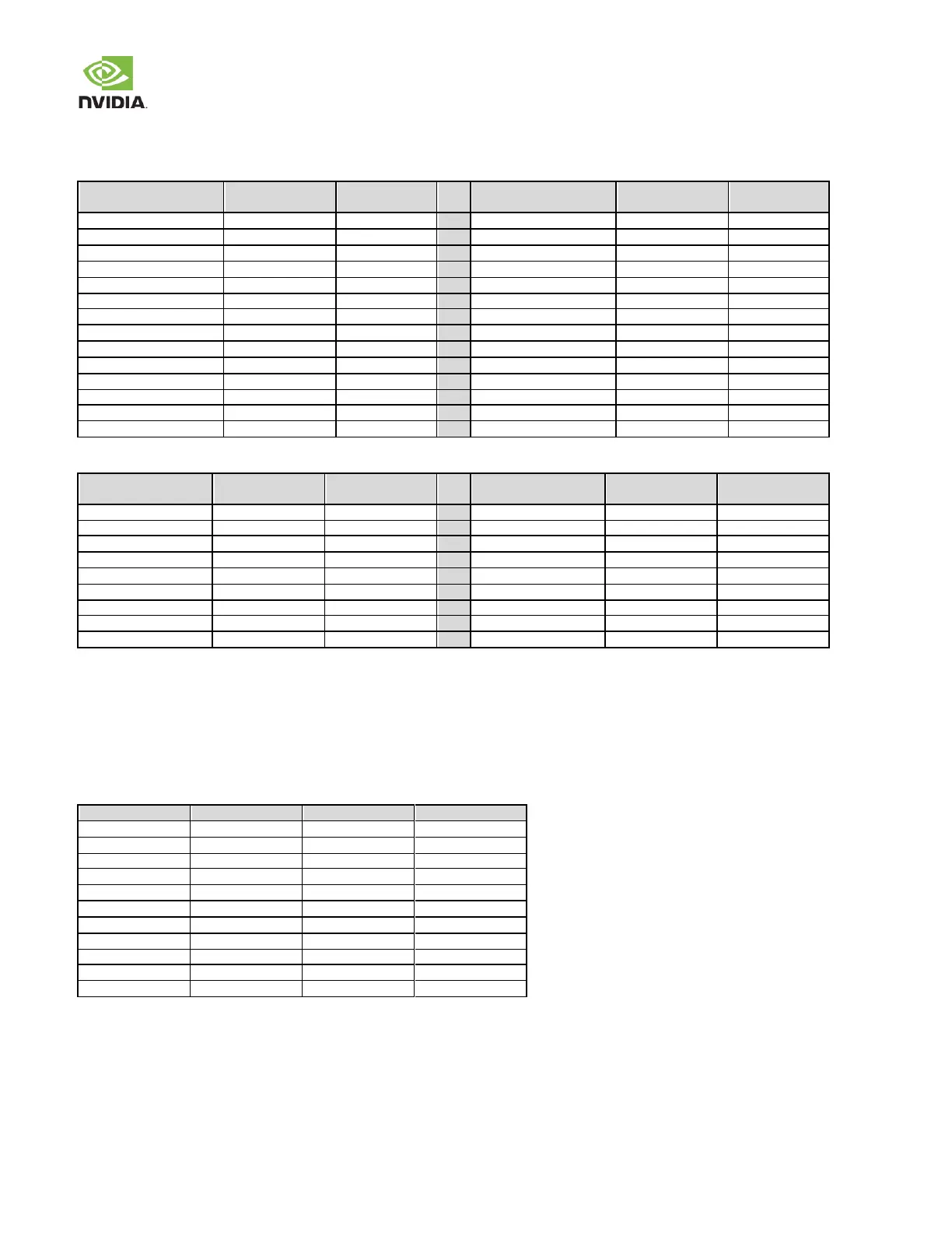
Table 87. Module Pins Pulled/Driven High by Tegra Prior to CARRIER_PWR_ON Active
Module Pin
Power-on Reset
Default
Pull-up Strength
(kΩ)
Module Pin
Power-on Reset
Default
Pull-up Strength
(kΩ)
DSPK_OUT_CLK
Internal Pull-up
~100
JTAG_TMS
Internal Pull-up
~100
SPI1_CS0#
Internal Pull-up
~100
JTAG_TDI
Internal Pull-up
~100
RESET_IN#
Driven High
na
UART1_RX
Internal Pull-up
~100
FORCE_RECOV#
Internal Pull-up
~100
SPI0_MISO
Internal Pull-up
~100
SLEEP#
Internal Pull-up
~100
SPI0_MOSI
Internal Pull-up
~100
GPIO7_TOUCH_RST
Driven High
na
CAN1_TX
Internal Pull-up
~20
CARRIER_STBY#
Driven High
na
CAN1_RX
Internal Pull-up
~20
GPIO5/CAM_FLASH_EN
Internal Pull-up
~100
CAN0_TX
Internal Pull-up
~20
USB0_VBUS_DET
Internal Pull-up
~100
CAN0_RX
Internal Pull-up
~20
SPI2_CS1#
Internal Pull-up
~100
GPIO6_TOUCH_INT
Driven High
na
SPI2_CS0#
Internal Pull-up
~100
GPIO3_CAM1_RST#
Internal Pull-up
~18
UART0_TX
Internal Pull-up
~100
CAM_VSYNC
Internal Pull-up
~18
UART0_RX
Internal Pull-up
~100
GPIO2_CAM0_RST#
Internal Pull-up
~18
WDT_TIME_OUT#
Driven High
na
Table 88. Module Pins Pulled High on the Module Prior to CARRIER_PWR_ON Active
Module Pin
Pull-up Supply
Voltage (V)
External
Pull-up (kΩ)
Module Pin
Pull-up Supply
Voltage (V)
External
Pull-up (kΩ)
VIN_PWR_BAD#
5.0
10
USB0_EN_OC#
3.3
100
RESET_OUT#
1.8
100
USB1_EN_OC#
3.3
100
I2C_GP0_CLK/DAT
1.8
1.0
PEX0_CLKREQ#
3.3
56
I2C_GP1_CLK/DAT
3.3
1.0
PEX0_RST#
3.3
56
I2C_GP2_CLK/DAT
1.8
1.0
PEX1_CLKREQ#
3.3
56
I2C_GP3_CLK/DAT
1.8
1.0
PEX1_RST#
3.3
56
I2C_PM_CLK/DAT
1.8
1.0
PEX2_CLKREQ#
3.3
56
I2C_CAM_CLK/DAT
1.8
1.0
PEX2_RST#
3.3
56
PEX_WAKE#
3.3
56
13.5 Pad Drive Strength
The table below provides the maximum MPIO pad output drive current w hen the pad is configured for the maximum
DRVUP/DRVDN values (11111b). The MPIO pad types include the ST, DD, CZ and LV_CZ type pads. The pad types can be
found in the Jetson TX2/TX2i Module Data Sheet.
Table 89. MPIO Maximum Output Drive Current
IOL/IOH
Pad Type
VOL
VOH
+/- 1mA
ST
0.15*VDD
0.825*VDD
+/- 1mA
DD
0.15*VDD
0.8*VDD
+/- 1mA
CZ (1.8V mode)
0.15*VDD
0.85*VDD
+/- 1mA
CZ (3.3V mode)
0.15*VDD
0.85*VDD
+/- 1mA
LV_CZ
0.15*VDD
0.85*VDD
+/- 2mA
ST
0.15*VDD
0.7*VDD
+/- 2mA
DD
0.175*VDD
0.7*VDD
+/- 2mA
CZ (1.8V mode)
0.25*VDD
0.75*VDD
+/- 2mA
CZ (3.3V mode)
0.15*VDD
0.75*VDD
+/- 2mA
LV_CZ
0.25*VDD
0.75*VDD

Other manuals for Nvidia JETSON TX2

Questions and Answers:

Question and Answer IconNeed help?

Do you have a question about the Nvidia JETSON TX2 and is the answer not in the manual?

Nvidia JETSON TX2 Specifications

General IconGeneral
BrandNvidia
ModelJETSON TX2
CategoryMicrocontrollers
LanguageEnglish

Related product manuals