NVIDIA Jetson TX2/TX2i OEM Product Design Guide
JETSON TX2/TX2i OEM PRODUCT | DESIGN GUIDE | 20180618 11
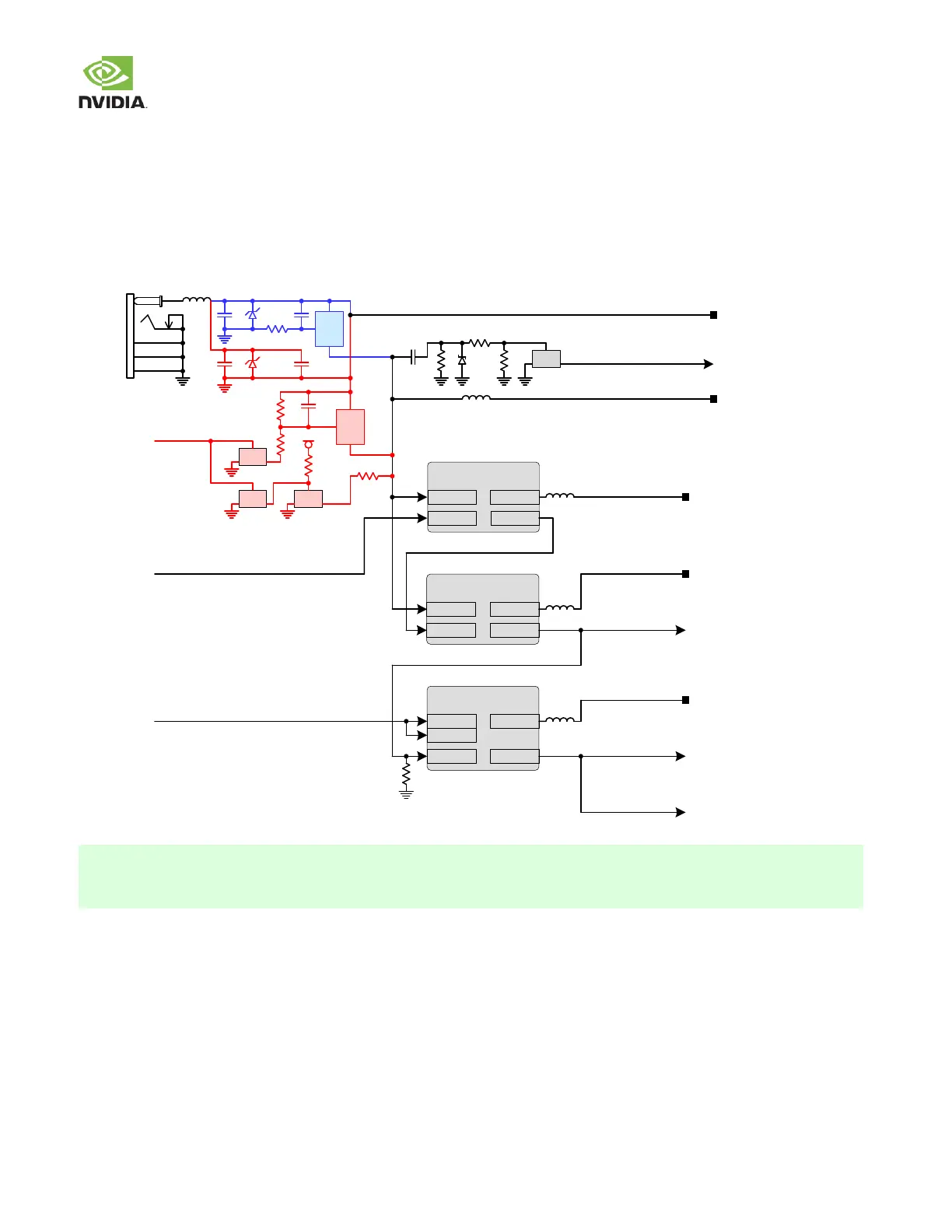
3.2 Main Power Sources/Supplies
The figure below shows the pow er connections used on the carrier board, including the DC Jack w hich connects to the AC/DC
adapter, and the main 5.0V, 3.3V and 1.8V supplies. Also show n are the pow er control signals that are used to enable these
supplies, or are used to communicate pow er sequence information to the module or other circuitry on the carrier board (i.e.
discharge circuits).
Figure 2. Main Power Source/Supply Connections
VDD_19V_IN (TX2: 5.5V-19.6V)
(TX2i: 9.0V-19.0V)
VIN_PWR_BAD#
VDD_MOD
TPS53015
DC-DC
SWVIN
CARRIER_PWR_ON
PGEN
3V3_SYS_BUCK_EN
TPS53015
DC-DC
SWVIN
PGEN
VDD_3V3_SYS_PG
VDD_3V3_SYS
To Jetson TX2 VDD_IN
From
Jetson TX2
To Jetson TX2 & Power
Discharge Circuitry
Main Carrier
Board 5V Supply
Main Carrier Board
3.3V Supply
Main 3.3V Power Good –
Routed to Power LED on
Carrier board
DC Jack
G
DS
FET
APW8805
OpenVReg
VIN SW
PGOOD
VDD_5V0_IO_SYS
VCC
1V8_IO_PG
EN/FS
VDD_1V8
1V8_IO_VREG_EN
RESET_OUT#
Main Carrier Board
1.8V Supply
To Jetson TX2 (RESET_OUT#)
to keep Tegra in Reset until
1.8V rail Valid
Main 3.3V Power Good –
Routed to Power LED on
Carrier board
From Main
5V supply
U31
U16
U9
VDD_5V0_IO_SYS
G
DS
FET
G
S
D
PWR
FET
G
S
D
PWR
FET
MOD_VIN_EN
G
DS
FET
G
DS
FET
5V
Red – P2597_C02
(TX2/TX2i)
Carrier Board
Blue – P2597_B04 Carrier Board
From On/Off
Controller
- The figure above is a high-level representation of the connections involved. Refer to the latest carrier board
reference design for details.
- When connecting the main power, the ground must make connection before the main power rail.
3.3 Power Sequencing
In order to ensure reliable and consistent pow er up sequencing, the pins VIN_PWR_BAD#, CARRIER_PWR_ON, and
RESET_OUT# on the module connector should be connected and used as described below :
VIN_PWR_BAD# signal is generated by the Carrier Board and passed to the module to keep the Tegra processor powered off
until the VDD_IN supply is stable and it is possible to pow er up any standby circuits on the module. This signal prevents the
Tegra processor from pow ering up prematurely before the Carrier Board has charged up its decoupling capacitors and pow er to
the module is stable