NVIDIA Jetson TX2/TX2i OEM Product Design Guide
JETSON TX2/TX2i OEM PRODUCT | DESIGN GUIDE | 20180618 87
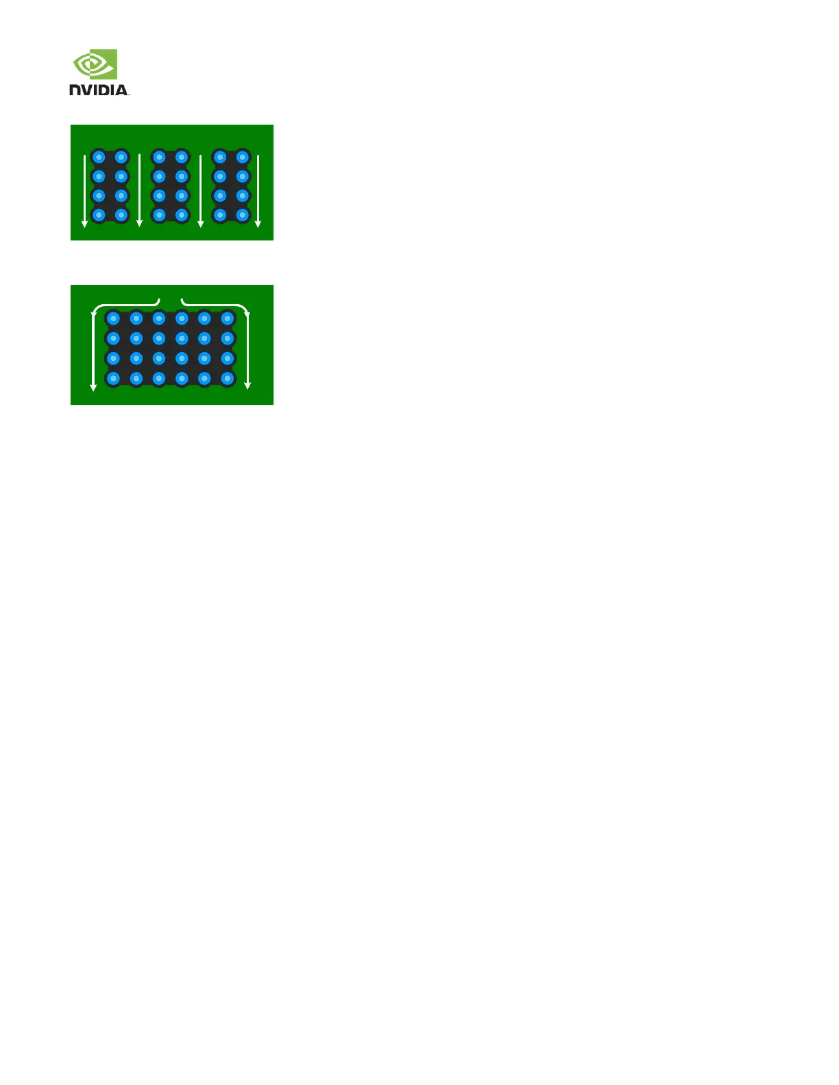
Figure 48. Good Current Flow Resulting from Correct Via Placement
In general, a dense via population should be avoided and good PCB design principles and analysis should be applied.
16.3 Connecting Vias
To be effective, vias must be connected properly to the signal and pow er planes. Poor via connections make the capacitor and
power planes less effective, leading to increased cost due to the need for additional capacitors to achieve equivalent
performance. This not only impacts the BOM (Bill of Material) cost of the design, but it can greatly impact quality and reliability of
the design.
16.4 Trace Guidelines
Trace length and impedance play a critical role in signal integrity betw een the driver and the receiver on the module. Signal
trace requirements are determined by the driver characteristics, source characteristics, and signal frequency of the propagating
signal.
16.4.1 Layer Stack-Up
The number of layers required is determined by the number of memory signal layers needed to achieve the desired
performance, and the number of power rails required to achieve the optimum pow er delivery/noise floor. For example, high-
performance boards require four memory signal routing layers, w ith at least tw o GND planes for reference. This comes to six
layers; add another tw o for pow er, w hich gives eight layers minimum. Reduction from eight to six layers starts the trade-off of
cost versus performance.
Pow er and GND planes usually serve tw o purposes in PCB design: power distribution and providing a signal reference for high-
speed signals.
Either the pow er or the ground planes can be used for high-speed signal reference; this is particularly common for low -cost
designs w ith a low layer count. When both power and GND are used for signal reference, make sure you minimize the reference
plane transition for all high-speed signals. Decoupling caps or transition vias should be added close to the reference plane
transitions.