NVIDIA Jetson TX2/TX2i OEM Product Design Guide
JETSON TX2/TX2i OEM PRODUCT | DESIGN GUIDE | 20180618 10
1. Power efficiency is higher when the input voltage is lower, such as 9V or 12V. At very low voltages (close to the 5.5V
minimum [TX2 only], the power supported by some of the supplies may be reduced).
2. These pins are handled as Open-Drain on the carrier board.
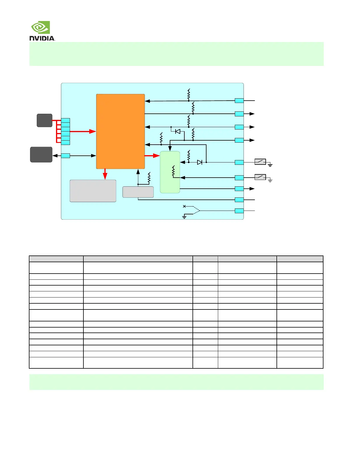
Figure 1. Power Block Diagram
Jetson TX2/TX2i
DC
Jack
A1
A2
B1
B2
C1
C2
A50
Memory/Peripherals
LPDDR4, eMMC,
Ethernet,
WiFi / BT (TX2 only)
Power Subsystem
5V/3.3V Pre-Regs
PMU Switchers/LDOs
CPU/GPU Regs
Ext. LDOs
Load Switches
Tegra
VDD_RTC
VDD_IN
B8
E2
B50
A47
A46
A48
VIN_PWR_BAD#
CARRIER_PWR_ON
RESET_IN#
RESET_OUT#
POWER_BTN#
SLEEP#
CARRIER_STBY#
CHARGER_PRSNT#
MOD_PWR_CFG_ID
B7
From Carrier Board main
power input & discharge circuit
To Carrier Board power subsystem
System Reset to/from Carrier Board
Tegra Force Reset from Carrier Board
Optional Sleep Button
To Carrier Board to disable devices/
rails to be off in sleep mode
SLEEP
Optional Power Button
POWER
Super Cap
or Li Cell
(Optional)
A49
Optional signal from Carrier Board
to support Auto-Power-On
PU
PU
PU
Auto-power-
on Circuit
PU
ACOK
PU
PU
PU
PU
B49
Jetson TX2
Jetson TX2i
To Carrier Board Power-on circuitry
(B49 on Jetson TX2 is RSVD – No Connect)
3.1 Supply Allocation
Table 6 Internal Power Subsystem Allocation
Supplies various switchers & load switches that power
the various circuits & peripherals on the module
Source for some DSI/CSI blocks
Supplies various LDOs & load switches that in turn
power the various circuits & peripherals on the module
Tegra Real Time Clock/Always-on Rail
Tegra PCIe / USB 3.0 / SATA rail
VDD_1V8_AP (&
VDD_1V8_AP_PLL)
This is the Tegra supply, and should not be confused with the module VDD_RTC pin which is the supply that connects to the
PMIC BBATT pin to keep the Real-Time Clock powered.