NVIDIA Jetson TX2/TX2i OEM Product Design Guide
JETSON TX2/TX2i OEM PRODUCT | DESIGN GUIDE | 20180618 78
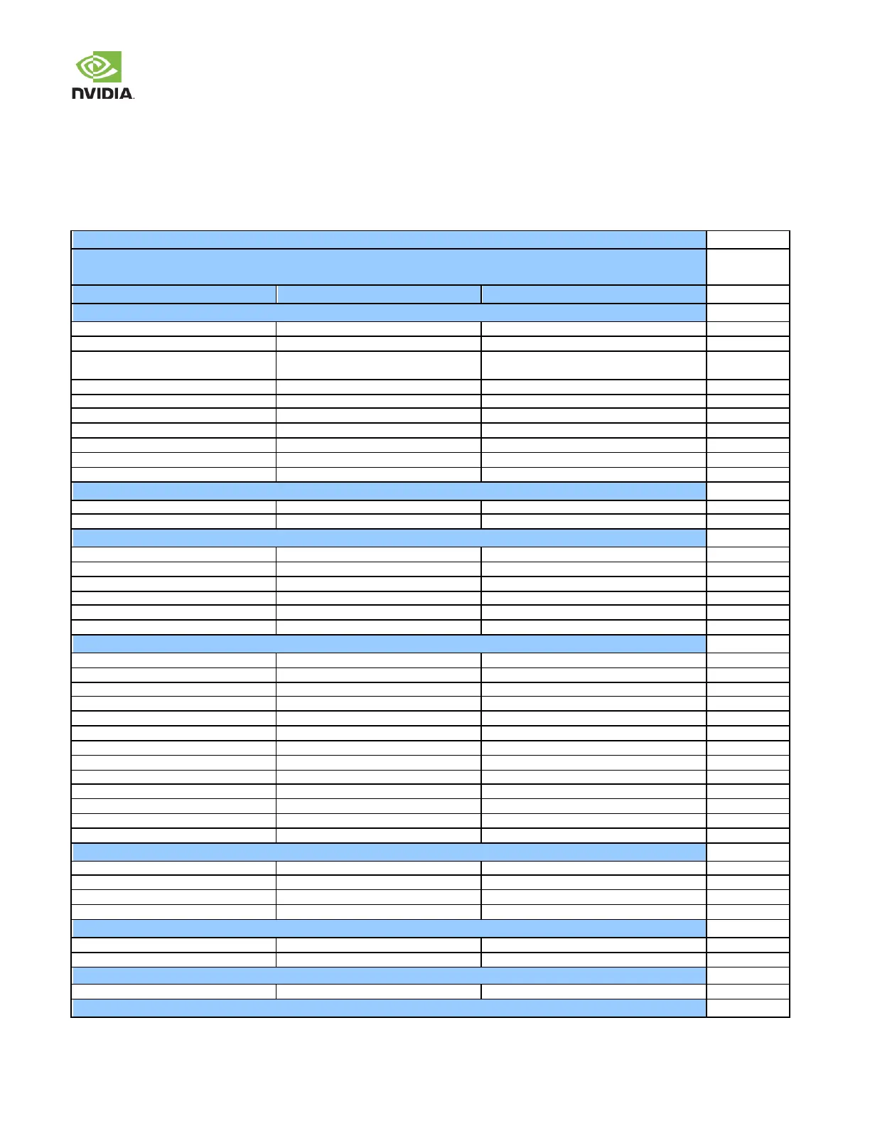
15.0 DESIGN CHECKLIST
The checklist below is intended to help ensure that the correct connections have been made in a design. The check items
describe connections for the various interfaces and the “Same/Diff/NA” column is intended to be used to indicate w hether the
design matches the check item description, is different, or is not applicable to the design.
Table 91. Checklist
Module Signal Terminations (Present on the module - shown for reference only)
Note: Internal refers to Tegra internal Pull-up/down resistors. External refers to resistors added on the module.
External 100K pull-up to 3.3V
External 100K pull-up to 3.3V
Level shifter between Tegra & the module
USB0_VBUS_DET pin
External 56K pull-up to 3.3V
External 56K pull-up to 3.3V
External 56K pull-up to 3.3V
External 56K pull-up to 3.3V
External 56K pull-up to 3.3V
External 56K pull-up to 3.3V
External 56K pull-up to 3.3V
External 1K pull-up to 1.8V
External 1K pull-up to 3.3V
External 1K pull-up to 1.8V
External 1K pull-up to 1.8V
External 1K pull-up to 1.8V
External 1K Pull Up to 1.8V
Internal pull-up to 1.8V/3.3V
Internal pull-up to 1.8V/3.3V