EasyManuals Logo
Home>Nvidia>Microcontrollers>JETSON TX2

Nvidia JETSON TX2 User Manual

Nvidia JETSON TX2
103 pages
To Next Page IconTo Next Page
To Previous Page IconTo Previous Page
Page #23 background imageLoading...
Page #23 background image
NVIDIA Jetson TX2/TX2i OEM Product Design Guide
JETSON TX2/TX2i OEM PRODUCT | DESIGN GUIDE | 20180618 23
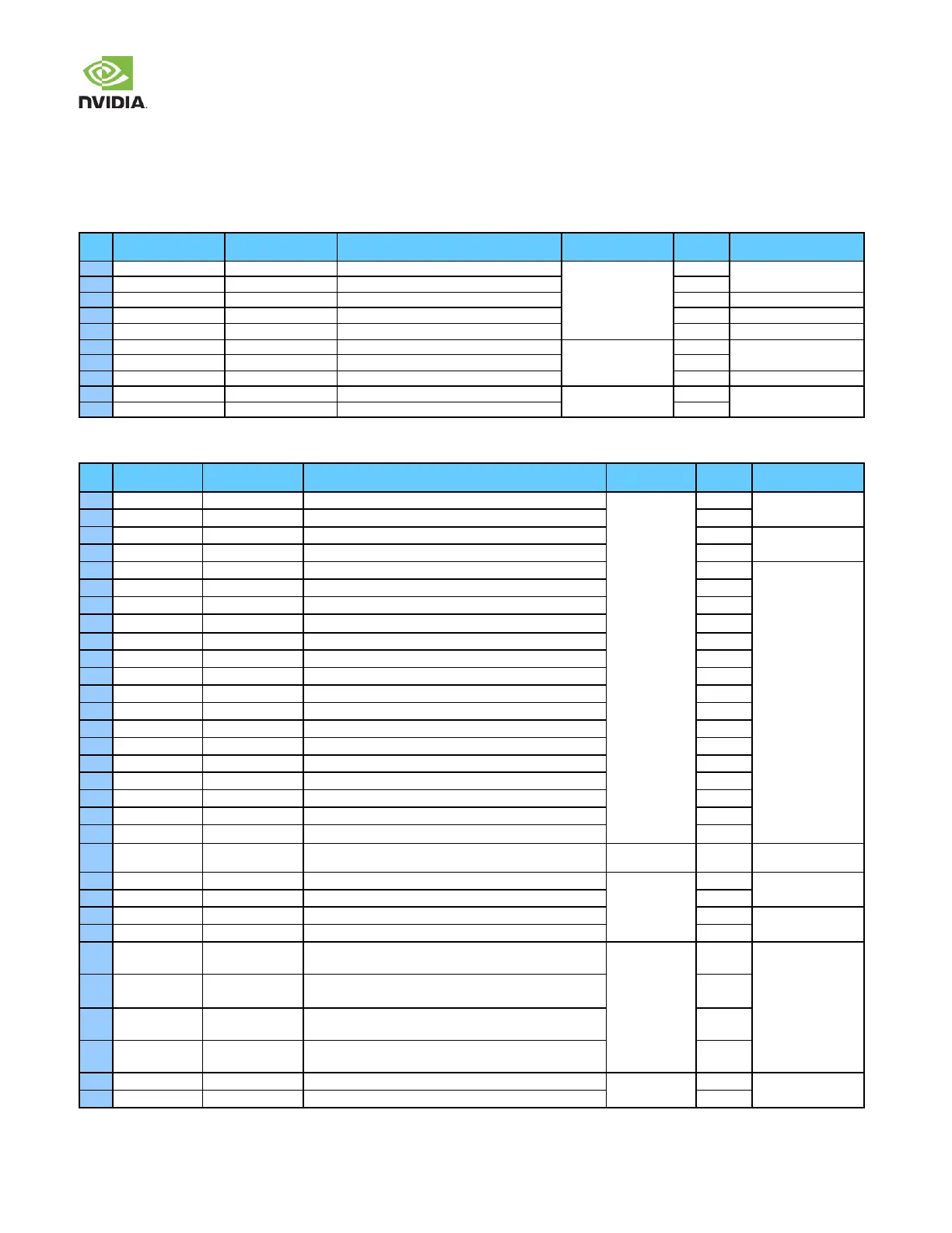
5.0 USB, PCIE & SATA
Jetson TX2/TX2i allow s multiple USB 3.0 & PCIe interfaces, and a single SATA interface to be brought out on the module. In
some cases, these interfaces are multiplexed on some of the module pins.
Table 13. USB 2.0 Pin Descriptions
Pin #
Module Pin Name
Tegra Signal
Usage/Description
Usage on Carrier
Board
Direction
Pin Type
B40
USB0_D
USB0_DN
USB 2.0 Port 0 Data
USB 2.0 Micro AB
Bidir
USB PHY
B39
USB0_D+
USB0_DP
USB 2.0 Port 0 Data+
Bidir
A17
USB0_EN_OC#
USB_VBUS_EN0
USB VBUS Enable/Overcurrent 0
Bidir
Open Drain 3.3V
A36
USB0_OTG_ID
(PMIC GPIO0)
USB 0 ID
Input
Analog
B37
USB0_VBUS_DET
UART5_CTS
USB 0 VBUS Detect
Input
USB VBUS, 5V
A39
USB1_D
USB1_DN
USB 2.0, Port 1 Data
USB 3.0 Type A
Bidir
USB PHY
A38
USB1_D+
USB1_DP
USB 2.0, Port 1 Data+
Bidir
A18
USB1_EN_OC#
USB_VBUS_EN1
USB VBUS Enable/Overcurrent 1
Bidir
Open Drain 3.3V
B43
USB2_D
USB2_DN
USB 2.0, Port 2 Data
M.2 Key E
Bidir
USB PHY
B42
USB2_D+
USB2_DP
USB 2.0, Port 2 Data+
Bidir
Table 14. USB 3.0, PCIe & SATA Pin Descriptions
Pin #
Module Pin
Name
Tegra Signal
Usage/Description
Usage on the
Carrier Board
Direction
Pin Type
A44
PEX0_REFCLK+
PEX_CLK1P
PCIe 0 Reference Clock+ (PCIe IF #0)
PCIe x4
Connector
Output
PCIe PHY
A45
PEX0_REFCLK
PEX_CLK1N
PCIe 0 Reference Clock (PCIe IF #0)
Output
C48
PEX0_CLKREQ#
PEX_L0_CLKREQ_N
PCIe 0 Clock Request (PCIe IF #0)
Bidir
Open Drain 3.3V, Pull-
up on the module
C49
PEX0_RST#
PEX_L0_RST_N
PCIe 0 Reset (PCIe IF #0)
Output
H44
PEX0_RX+
PEX_RX4P
PCIe 0 Lane 0 Receive+ (PCIe IF #0)
Input
PCIe PHY, AC-Coupled
on carrier board
H45
PEX0_RX
PEX_RX4N
PCIe 0 Lane 0 Receive (PCIe IF #0)
Input
E44
PEX0_TX+
PEX_TX4P
PCIe 0 Lane 0 Transmit+ (PCIe IF #0)
Output
E45
PEX0_TX
PEX_TX4N
PCIe 0 Lane 0 Transmit (PCIe IF #0)
Output
G42
USB_SS1_RX+
PEX_RX2P
USB SS 1 Receive+ (USB 3.0 Port #2 or PCIe IF #0 Lane 1)
Input
G43
USB_SS1_RX
PEX_RX2N
USB SS 1 Receive (USB 3.0 Port #2 or PCIe #0 Lane 1)
Input
D42
USB_SS1_TX+
PEX_TX2P
USB SS 1 Transmit+ (USB 3.0 Port #2 or PCIe IF #0 Lane 1)
Output
D43
USB_SS1_TX
PEX_TX2N
USB SS 1 Transmit (USB 3.0 Port #2 or PCIe #0 Lane 1)
Output
F40
PEX2_RX+
PEX_RX3P
PCIe 2 Receive+ (PCIe IF #0 Lane 2 or PCIe IF #1 Lane 0)
Input
F41
PEX2_RX
PEX_RX3N
PCIe 2 Receive (PCIe IF #0 Lane 2 or PCIe IF #1 Lane 0)
Input
C40
PEX2_TX+
PEX_TX3P
PCIe 2 Transmit+ (PCIe IF #0 Lane 2 or PCIe IF #1 Lane 0)
Output
C41
PEX2_TX
PEX_TX3N
PCIe 2 Transmit (PCIe IF #0 Lane 2 or PCIe IF #1 Lane 0)
Output
G39
PEX_RFU_RX+
PEX_RX1P
PCIe RFU Receive+ (PCIe IF #0 Lane 3 or USB 3.0 Port #1)
Input
G40
PEX_RFU_RX
PEX_RX1N
PCIe RFU Receive (PCIe IF #0 Lane 3 or USB 3.0 Port #1)
Input
D39
PEX_RFU_TX+
PEX_TX1P
PCIe RFU Transmit+ (PCIe IF #0 Lane 3 or USB 3.0 Port #1)
Output
D40
PEX_RFU_TX
PEX_TX1N
PCIe RFU Transmit (PCIe IF #0 Lane 3 or USB 3.0 Port #1)
Output
D48
PEX_WAKE#
PEX_WAKE_N
PCIe Wake
PCIe x4 conn &
M.2
Input
Open Drain 3.3V, Pull-
up on the module
B45
PEX1_REFCLK+
PEX_CLK3P
PCIe Reference Clock 1+ (PCIe IF #2)
M.2 Key E
Output
PCIe PHY
B46
PEX1_REFCLK
PEX_CLK3N
PCIe Reference Clock 1 (PCIe IF #2)
Output
C47
PEX1_CLKREQ#
PEX_L2_CLKREQ_N
PCIE 1 Clock Request (mux option - PCIe IF #2)
Bidir
Open Drain 3.3V, Pull-
up on the module
E50
PEX1_RST#
PEX_L2_RST_N
PCIe 1 Reset (PCIe IF #2)
Output
H41
PEX1_RX+
PEX_RX0P
PCIe 1 Receive+ (PCIe #2 Lane 0 muxed w/USB 3.0 Port
#0)
USB 3.0 Type A
(Default) or M.2
Key E
Input
PCIe PHY, AC-Coupled
on carrier board
H42
PEX1_RX
PEX_RX0N
PCIe 1 Receive (PCIe #2 Lane 0 muxed w/USB 3.0 Port
#0)
Input
E41
PEX1_TX+
PEX_TX0P
PCIe 1 Transmit+ (PCIe #2 Lane 0 muxed w/USB 3.0 Port
#0)
Output
E42
PEX1_TX
PEX_TX0N
PCIe 1 Transmit (PCIe #2 Lane 0 muxed w/USB 3.0 Port
#0)
Output
A41
PEX2_REFCLK+
PEX_CLK2P
PCIe 2 Reference Clock+ (PCIe IF #1)
Unassigned
Output
PCIe PHY
A42
PEX2_REFCLK
PEX_CLK2N
PCIe 2 Reference Clock (PCIe IF #1)
Output

Other manuals for Nvidia JETSON TX2

Questions and Answers:

Question and Answer IconNeed help?

Do you have a question about the Nvidia JETSON TX2 and is the answer not in the manual?

Nvidia JETSON TX2 Specifications

General IconGeneral
BrandNvidia
ModelJETSON TX2
CategoryMicrocontrollers
LanguageEnglish

Related product manuals