NVIDIA Jetson TX2/TX2i OEM Product Design Guide
JETSON TX2/TX2i OEM PRODUCT | DESIGN GUIDE | 20180618 25
Table 16. USB 3.0, PCIe & SATA Lane Mapping Configurations compatible with Jetson TX2 & Jetson TX2i only.
Avail. Outputs from the
module
Default Usage on CB (carrier board)
6. PCIe interface #2 can be brought to the PEX1 pins, or USB 3.0 port #1 to the USB_SS0 pins on Jetson TX2/TX2i depending
on the setting of a multiplexor on the module. The selection is controlled by QSPI_IO2 configured as a GPIO.
7. Jetson TX2/TX2i has been designed to enable use cases listed in the table above. However, released Software may not
support all configurations, nor has every configuration been validated.
o Configuration #1 & 2 represent the supported and validated Jetson TX2/TX2i Developer Kit configurations. These
configurations are supported by the released Software, and the PCIe, USB 3.0, and SATA interfaces have been
verified on the carrier board.
8. See notes under the Backward Compatible mapping table related to color coding, PCIe x2/x1 support & lane reversal.
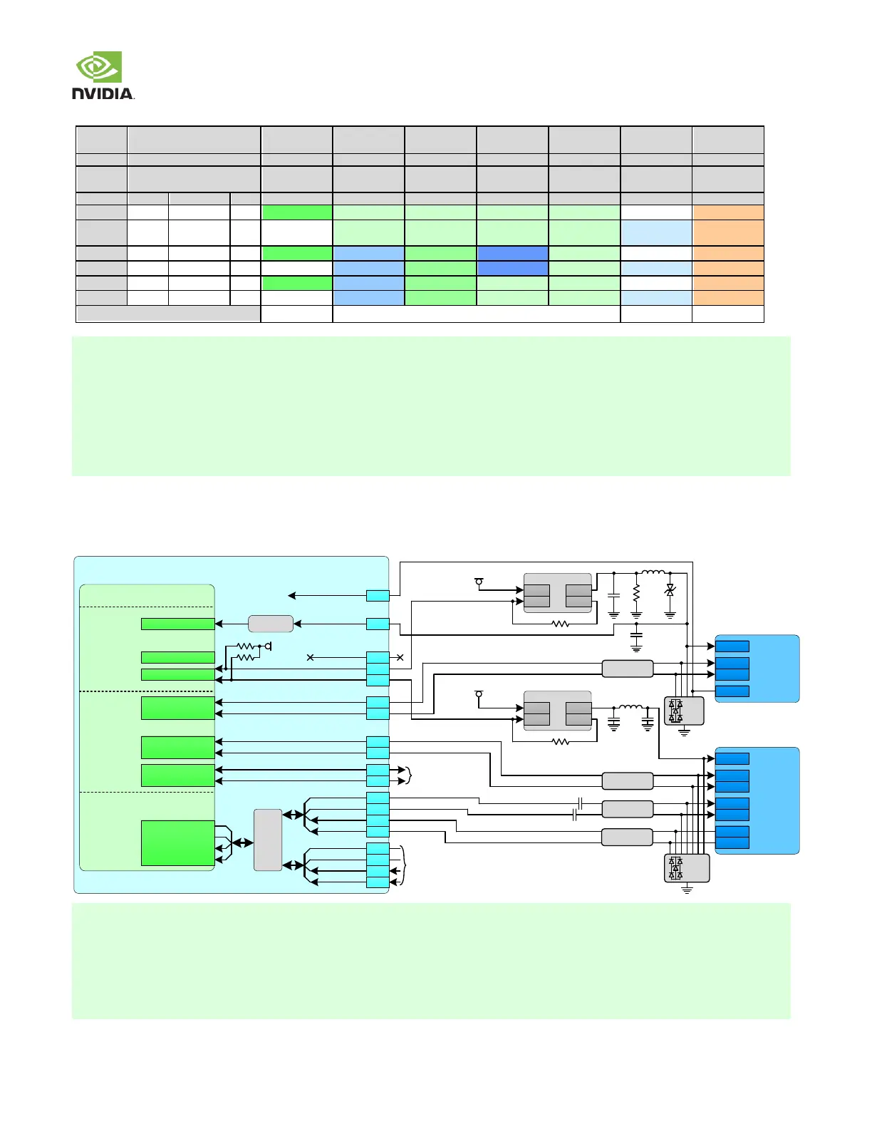
5.1 USB
Figure 15 USB 2.0 OTG + USB 3.0 Host Connection Example
Jetson TX2/TX2i
USB 3.0
Type A
USB 2.0
Micro AB
VBUS
ID
D+
D–
VBUS
TX+
D+
D–
TX–
RX+
RX–
USB_VBUS_EN0
Tegra
USB 2.0
USB0_DP
USB0_DN
USB 3.0
& PEX
USB1_DP
USB1_DN
USB2_DP
USB2_DN
ESD
ESD
Common
Mode Choke
Load Switch
EN OC
IN OUT
VDD_5V0_IO_SYS
USB_VBUS_EN1
Load Switch
EN OC
IN OUT
VDD_5V0_IO_SYS
Common
Mode Choke
Common
Mode Choke
USB0_D+
USB0_D
USB1_D+
USB1_D
USB2_D+
USB2_D
USB_SS0_TX+
USB_SS0_TX
USB_SS0_RX+
USB_SS0_RX
PEX1_TX+
PEX1_TX
PEX1_RX+
PEX1_RX
USB0_OTG_ID
USB0_VBUS_DET
USB2_EN_OC#
USB0_EN_OC#
USB1_EN_OC#
Gate/LS
To PMIC G PIO0
(o n Module)
VDD_3V3_SYS
To M.2 Module
on Carrier Board
A36
A17
A18
B3 9
B3 7
B4 0
A38
A39
B4 2
B4 3
C43
C44
F43
F44
A19
0.1uF
0.1uF
100kΩ
PEX_TX0_P
PEX_TX0_N
PEX_RX0_P
PEX_RX0_N
UART5_CTS_N
UARTCAM
USB_VBUS_EN0
USB_VBUS_EN1
Common
Mode Choke
Mux
PCIe#2 (x1)
Default
100Ω
100Ω
E41
E42
H41
H42
1. Common mode filters on USB[2:0]_DP/DN (USB 2.0 interfaces) are optional. Place only as needed if EMI is an issue.
Common mode filters on USB3_TX/RX_P/N signals are not recommended. If common mode devices are placed, they
must be selected to minimize the impact to signal quality, which must meet the USB spec. signal requirements. See the
Common Mode Choke requirements in the USB 3.0 Interface Signal Routing Requirements table .
2. If USB 3.0 is routed to a connector, only AC caps on the module TX lines are required. If routed directly to a peripheral,
AC caps are needed for both the module TX lines (connected to device RX) & Device TX lines (connected to the module
RX).