NVIDIA Jetson TX2/TX2i OEM Product Design Guide
JETSON TX2/TX2i OEM PRODUCT | DESIGN GUIDE | 20180618 26
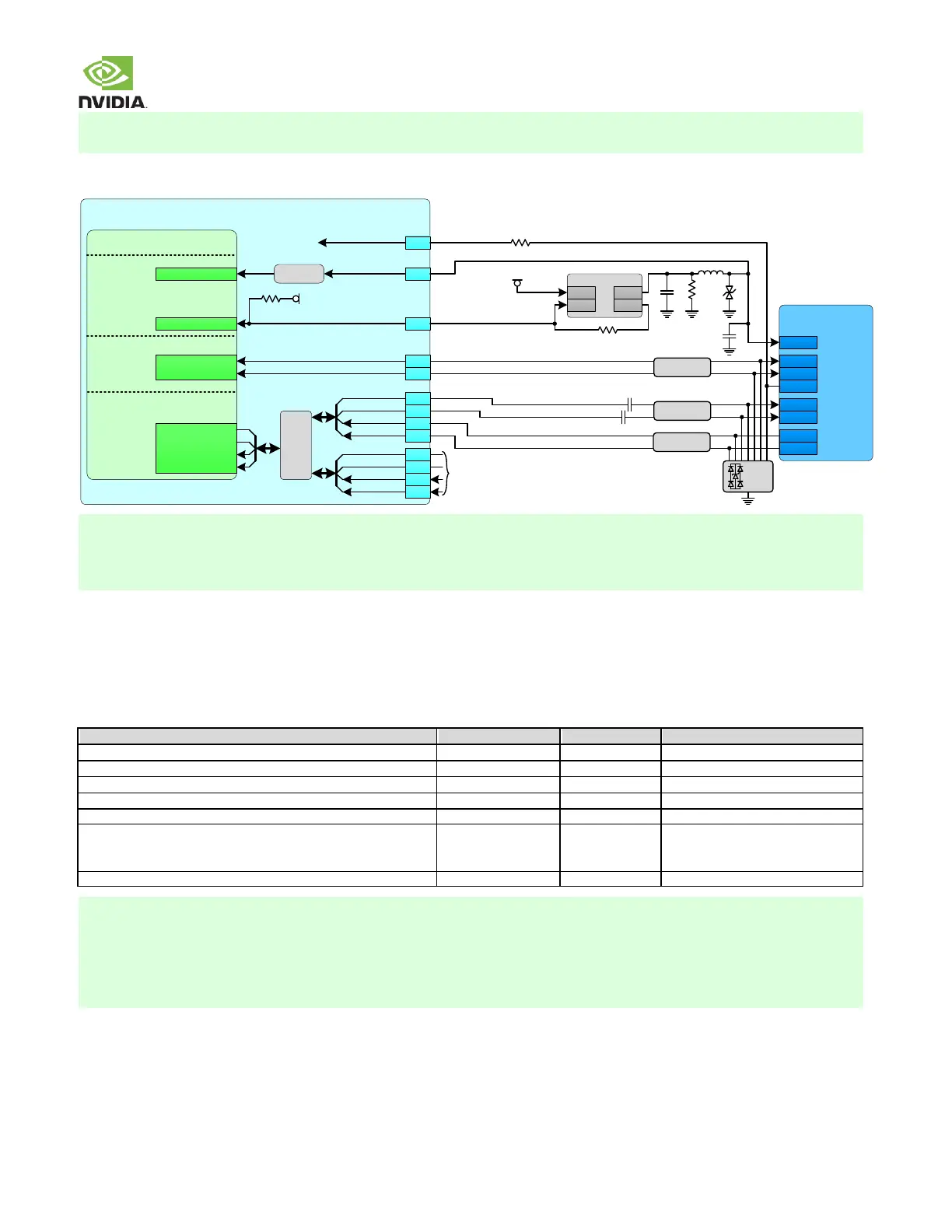
3. USB0 must be available to use as USB Device for USB Recovery Mode.
4. Connector used must be USB-IF certified if USB 3.0 implemented.
Figure 16 USB 2.0/3.0 Dual-mode (host/device) Connection Example
Jetson TX2/TX2i
USB 3.0
Micro AB
VBUS
TX+
D+
D–
TX–
RX+
RX–
Tegra
USB 2.0
USB0_DP
USB0_DN
USB 3.0
& PEX
ESD
Common
Mode Choke
Common
Mode Choke
USB0_D+
USB0_D
USB_SS0_TX+
USB_SS0_TX
USB_SS0_RX+
USB_SS0_RX
PEX1_TX+
PEX1_TX
PEX1_RX+
PEX1_RX
USB0_OTG_ID
USB0_VBUS_DET
USB0_EN_OC#
Gate/LS
To PMIC GPIO0
(on Module)
VDD_3V3_SYS
A36
A17
B3 9
B3 7
B4 0
C43
C44
F43
F44
0.1uF
0.1uF
PEX_TX0_P
PEX_TX0_N
PEX_RX0_P
PEX_RX0_N
UART5_CTS_N
UARTCAM
USB_VBUS_EN0
Common
Mode Choke
Mux
PCIe#2 (x1)
Default
100Ω
E41
E42
H41
H42
ID
USB_VBUS_EN0
Load Switch
EN OC
IN OUT
VDD_5V0_IO_SYS
100kΩ
100Ω
1. See notes under USB 2.0 OTG + USB 3.0 Host Connection Example figure.
2. USB 3.0 Port #0 is shown in the example above. Other supported USB 3.0 ports can be used instead. As noted, USB0
must be routed to a connector to support USB recovery mode. Since the connector above would be the only Device
capable connector in the system connected to Tegra, USB0 must be used.
USB 2.0 Design Guidelines
These requirements apply to the USB 2.0 controller PHY interfaces: USB[2:0]_D/D+
Table 17. USB 2.0 Interface Signal Routing Requirements
Max Frequency (High Speed) Bit Rate/UI period/Frequency
Max Loading High Speed / Full Speed / Low Speed
Trace Impedance Diff pair / Single Ended
Via proximity (Signal to reference)
Max Trace Delay With CMC or SW (Microstrip / Stripline)
Without CMC or SW (Microstrip / Stripline)
900/1050 (6)
1350/1575 (9)
Prop delay assumption: 175ps/in.
for stripline, 150ps/in. for
microstrip). See Note 3
Max Intra-Pair Skew between USBx_D+ & USBx_D–
1. If portion of route is over a flex cable this length should be included in the Max Trace Delay/Length calculation & 85
Differential pair trace impedance is recommended.
2. Up to 4 signal Vias can share a single GND return Via.
3. CMC = Common-Mode-Choke. SW = Analog Switch
4. Adjustments to the USB drive strength, slew rate, termination value settings should not be necessary, but if any are
made, they MUST be done as an offset to default values instead of overwriting those values.