NVIDIA Jetson TX2/TX2i OEM Product Design Guide
JETSON TX2/TX2i OEM PRODUCT | DESIGN GUIDE | 20180618 27
USB 3.0 Design Guidelines
The follow ing requirements apply to the USB 3.0 PHY interfaces
Table 18. USB 3.0 Interface Signal Routing Requirements
On-die termination at TX & RX
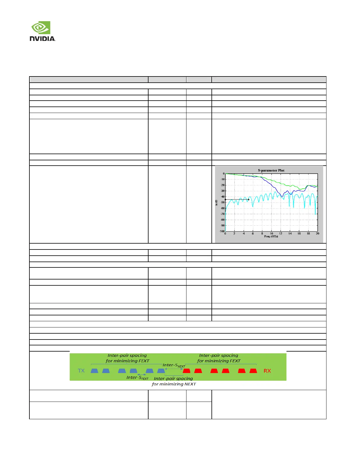
Insertion Loss (IL)
Host Type C
Type A
Device Micro AB
Resonance Dip Frequency
@ 2.5GHz
@ 2.5GHz
@ 2.5GHz
The resonance dip could be caused by a via stub for
layer transition or trace stub for co-layout.
Using TDR pulse with Tr (10%-90%) = 200ps
Near-end Crosstalk (NEXT) @ DC to 5GHz
Trace Impedance Diff pair / Single Ended
Trace loss characteristic @ 2.5GHz
The following max length is derived based on this
characteristic. See Note 1.
Breakout Region Max trace length/delay
Trace with minimum width and spacing
Max PCB Trace Length
Host
Device
Max Within Pair (Intra-Pair) Skew
Do trace length matching before hitting discontinuities
Differential pair uncoupled length
Trace Spacing – for TX/RX non-interleaving
TX-RX Xtalk is very critical in PCB trace routing. The ideal solution is to route TX and RX on different layers.
If routing on the same layer, strongly recommend not interleaving TX and RX lanes
If it is necessary to have interleaved routing in breakout, all the inter-pair spacing should follow the rule of inter-SNEXT
The breakout trace width is suggested to be the minimum to increase inter-pair spacing
Do not perform serpentine routing for intra-pair skew compensation in the breakout region
Min Inter-S
NEXT
Breakout
(between TX/RX) Main-route
- This is the recommended dimension for meeting
NEXT requirement
- This is the recommended dimension for meeting
NEXT requirement
Min Inter-S
FEXT
Breakout
(between TX/TX or RX/RX)
Main-route