NVIDIA Jetson TX2/TX2i OEM Product Design Guide
JETSON TX2/TX2i OEM PRODUCT | DESIGN GUIDE | 20180618 28
- Stripline structure in a GSSG structure is assumed; it
holds in broadside-coupled stripline structure
- All v alues are in terms of minimum dielectric height
Max length Breakout
Main-route
11
Max trace
length - LBRK
Trace Spacing – for TX/RX interleaving
Trace Spacing
Pair-Pair (inter-pair) Microstrip / Stripline
To plane & capacitor pad Microstrip / Stripline
To unrelated high-speed signals Microstrip / Stripline
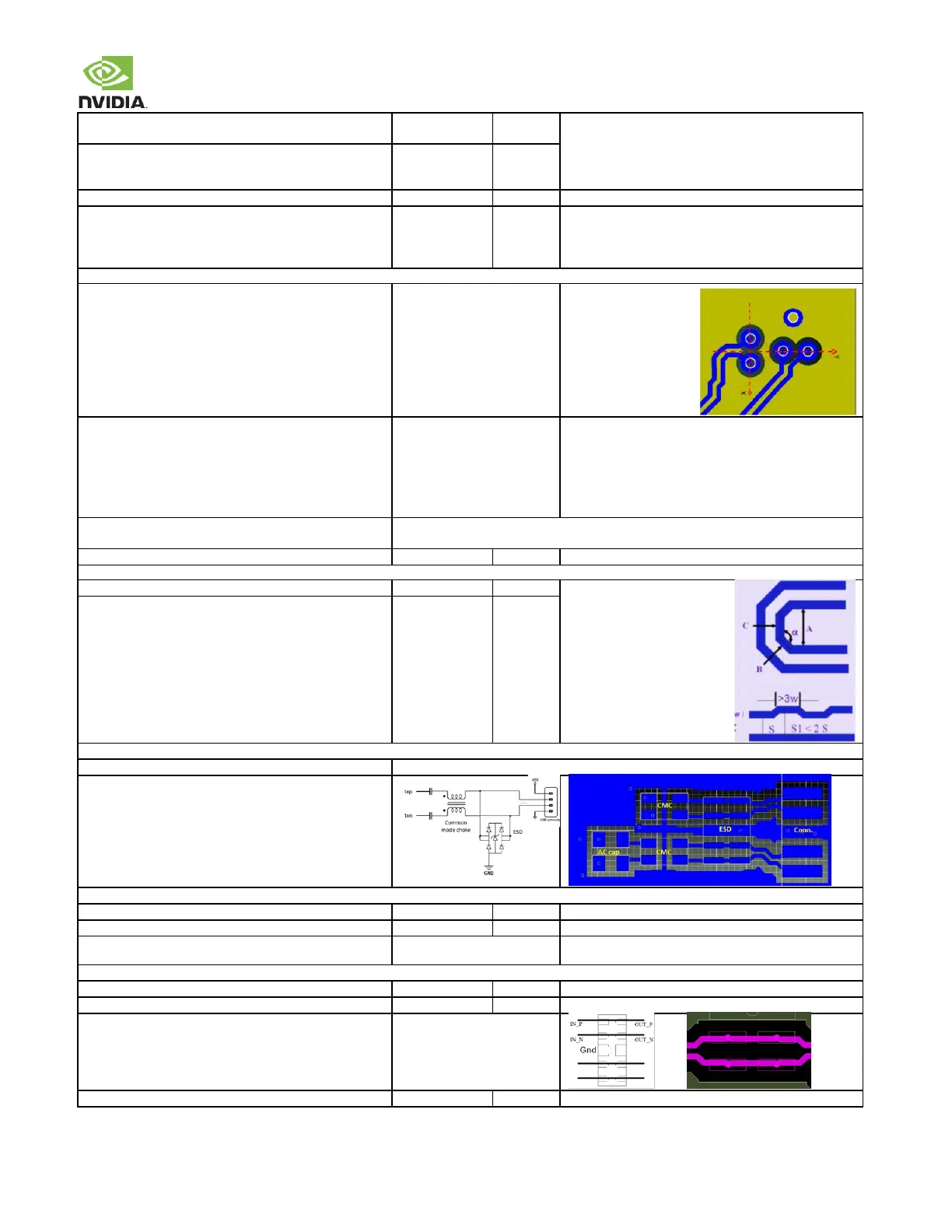
- Y-pattern is
recommended
- Keep symmetry
Y-pattern helps with
Xtalk suppression. It
can also reduce the
limit of pair-pair
distance. Need review
(NEXT/FEXT check) if
via placement is not Y-
pattern.
- Place ground vias as
sy mmetrically as
possible to data pair
vias
- up to 4 signal v ias (2
diff pairs) can share a
single GND return via
GND via is used to maintain return path, while its Xtalk
suppression is limited
Max # of Vias PTH vias
Micro Vias
4
Not limited as long as total channel loss meets IL spec
long via stub requires review (IL & resonance dip check)
S1 must be taken care in order
to consider Xtalk to adjacent
pair
Dimension Min A Spacing
Min B, C Length
Min Jog Width
Chip AC capacitor (TX only) common mode choke ESD Connector
Only required for TX pair when routed to connector
Location (max length to adjacent discontinuity)
Discontinuity is connector, via, or component pad
GND/PWR void under/above
cap is preferred
Voiding is required if AC cap size is 0603 or larger
ESD (the usage of ESD is optional. A design should include the footprint for ESD as a stuffing option)
Max Junction capacitance (IO to GND)
Pad should be on the net
not trace stub
Location (max length to adjacent discontinuity)
Discontinuity is connector, via, or component pad