104
PULSE OUTPUT: PLS2(887) Section 5-7
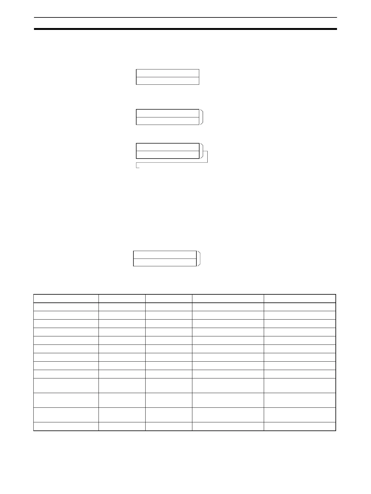
S: First Word of Settings Table
The contents of S to S+5 control the pulse output as shown in the following
diagrams.
The actual number of movement pulses that will be output are as follows:
For relative pulse output, the number of movement pulses = the set number of
pulses. For absolute pulse output, the number of movement pulses = the set
number of pulses
− the PV.
F: First Word of Starting Frequency
The starting frequency is given in F and F+1.
Operand Specifications
S1+4
S1+5
S1+2
S1+3
S1
S1+1
0
15
Lower word with number of output pulses
Upper word with number of output pulses
Relative pulse output: 0 to 2,147,483,647
(0000 0000 to 7FFF FFFF hex)
Absolute pulse output: -2,147,483,648 to 2,147,483,647
(8000 0000 to 7FFF FFFF hex)
Lower word with target frequency
Upper word with target frequency
1 to 100,000 Hz
(0000 0000 to 0001 86A0 hex)
Specify the frequency after acceleration in Hz.
Acceleration rate
Deceleration rate
Specify the increase or decrease in the frequency per pulse control period (4 ms).
• CJ1M Pre-Ver. 2.0 CPU Units
1 to 2,000 Hz (0001 to 07D0 hex)
• CJ1M CPU Units Ver. 2.0
1 to 65,535 Hz (0001 to FFFF hex)
F
F+1
0
15
Lower word with starting frequency
Upper word with starting frequency
0 to 100,000 Hz
(0000 0000 to 0001 86A0 hex)
Specify the starting frequency in Hz.
Area P M S F
CIO Area --- --- CIO 0000 to CIO 6138 CIO 0000 to CIO 6142
Work Area --- --- W000 to W506 W000 to W510
Holding Bit Area --- --- H000 to H506 H000 to H510
Auxiliary Bit Area --- --- A000 to A954 A000 to A958
Timer Area --- --- T0000 to T4090 T0000 to T4094
Counter Area --- --- C0000 to C4090 C0000 to C4094
DM Area --- --- D00000 to D32762 D00000 to D32766
EM Area without bank --- --- --- ---
EM Area with bank --- --- --- ---
Indirect DM/EM
addresses in binary
--- --- @ D00000 to @ D32767 @ D00000 to @ D32767
Indirect DM/EM
addresses in BCD
--- --- *D00000 to *D32767 *D00000 to *D32767
Constants See description
of operand.
See description
of operand.
--- See description of oper-
and.
Data Registers --- --- --- ---