136
Analog Output Units Section 5-2
Output Status after
Communications Error
Pins 8 and 9 of the DIP switch determine the status of the outputs after a com-
munications error occurs in DeviceNet or I/O Unit interface communications.
When the clear to minimum, clear to maximum, or clear to 0 V setting is used,
the output data is as shown in the following table.
Converted Data Output the converted data to the Master as shown in the following diagram.
When a negative voltage is to be output, specify the conversion data as the
two’s complement. To obtain a two’s complement from an absolute value, the
NEG instruction is useful.
Conversion Time The conversion data is refreshed every 4 ms for all 4 points.
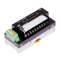
Dimensions
Note The vertical center of the Unit is 4.9 mm lower than the center of the DIN
track. The Unit therefore extends downward 41.4 mm (including the mounting
hook) from the DIN track center.
Settings Output status after communications error
Pin 8 Pin 9
OFF OFF Clear to minimum (Clear to the lower limit of the output signal
range.)
OFF ON Clear to maximum (Clear to the upper limit of the output signal
range.)
ON OFF Clear to 0 V (for –10 to 10 V only)
Clear to minimum (other than the above)
ON ON Hold (Maintain previous output status.)
Output signal range Clear to minimum Clear to maximum Clear to 0 V
0 to 5 V –0.25 V 5.25 V –0.25 V
1 to 5 V 0.8 V 5.2 V 0.8 V
0 to 10 V –0.5 V 10.5 V –0.5 V
–10 to 10 V –11 V 11 V 0 V
Bit
First word
First word + 1
First word + 2
First word + 3
Output 0 data
Output 1 data
Output 2 data
Output 3 data
(Unit: mm)
Approx. 70
110
60
65
37.4
27.6
4
35
12.6