IC BLOCK DIAGRAMS AND TERMINAL DESCRIPTIONS -45
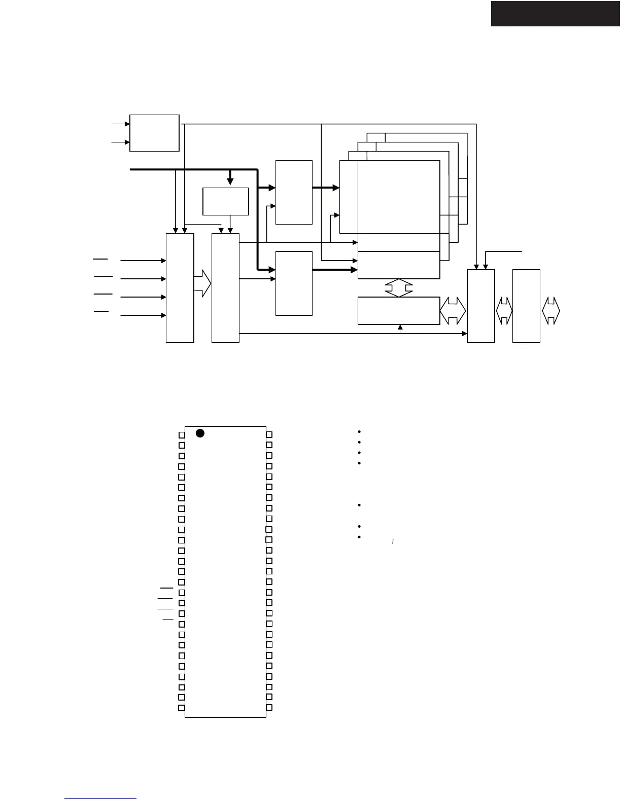
BLOCK DIAGRAM
PIN CONFIGURATION
Q3661:M12L64164A-7TG (64 Mbit Syncronous DRAM)
TX-SR876/SA876
L(U)DQM
DQ
Mode
Register
Control Logic
Column
Address
Buffer
&
Refresh
Counter
Row
A
ddress
Buffer
&
Refresh
Counter
Bank D
Row Decoder
Bank A
Bank B
Bank C
Sense Amplifier
Column Decoder
Data Control Circuit
Latch Circuit
Input & Output
Buffer
Address
Clock
Generator
CLK
CKE
Command Decoder
CS
RAS
CAS
WE
Top View
1
2
3
4
5
6
7
8
9
10
11
12
13
14
15
16
17
18
19
20
21
22
23
24
25
26
27
V
DD
DQ0
V
DDQ
DQ1
DQ2
V
SSQ
DQ3
DQ4
V
DDQ
DQ5
DQ6
V
SSQ
DQ7
V
DD
LDQM
WE
CAS
RAS
CS
A
13
A12
A10/AP
A
0
A1
A2
A3
VDD
54
53
52
51
50
49
48
47
46
45
44
43
42
41
40
39
38
37
36
35
34
33
32
31
30
29
28
V
SS
DQ15
V
SSQ
DQ14
DQ13
V
DDQ
DQ12
DQ11
V
SSQ
DQ10
DQ9
V
DDQ
DQ8
V
SS
NC
UDQM
CLK
CKE
NC
A
11
A9
A8
A7
A6
A5
A4
VSS
FEATURES
JEDEC standard 3.3V power supply
LVTTL compatible with multiplexed address
Four banks operation
MRS cycle with address key programs
- CAS Latency (2 & 3)
- Burst Length (1, 2, 4, 8 & full page)
- Burst Type (Sequential & Interleave)
All inputs are sampled at the positive going edge
of the system clock
Auto & self refresh
15.6 us refresh interval
 Loading...