6-- 5
Powerware 9315 (500 kVA--750 kVA) T1 and T3 Installation Addendum
164201244--001 REV. A 011500
6.3.2 Multi-Module Preparation
To install a multi-module UPS system using a System Bypass Module, perform the
procedures in the following paragraphs.
6.3.2.1 Installing UPS Internal Power and Control Wiring
NOTE: The cables used in steps 3 through 5 are coiled inside the Input/Rectifier
cabine t and are attached at the factory to the output of the rectifier.
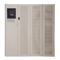
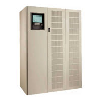
1. Position UPS cabinet sections side by side (Input /Rectifier cabinet on the left
and Output/Inverter on the right).
2. Remove the plastic shield covering the inverter input section of the
Output/Inverter cabinet.
3. Route DC Link cables from the rectifier output (Input/Rectifier cabinet) through
cutout in cabinet sides to the inverter input (Output/Inverter cabinet) .
4. Connect positive DC Link power wiring to the inverter input. Connect two
cables to each inverter. Refer to Appendix A of the referenced installation
manual for terminal locations and tightening torque.
5. Connect negative DC Link pow er wiring to the inverter input. Connect two
cables to each inverter. Refer to Appendix A of the referenced installation
manual for terminal locations and tightening torque.
6. Reinstall inverter input section plastic shield.
7. Route ground braid from top of Output/Inverter cabinet to Input/Rectifier
cabinet through cabinet cutouts. Braid is secured at the factory to the
Output/Inverter cabinet mounting stud.
8. Connect ground braid to Input/Rectifier cabinet mounting stud and secure.
9. Connect the Output/Inverter 15-pin control wiring harness connector P100 to
the Input/Rectifier 15-pin control wiring harness connector J100. Refer to
Appendix A of the referenced installation manual for connector locations.
10. Reinstall inverter output section plastic shield.
6.3.2.2 Multi- Module Test Setup
1. Verify all fuses are installed.
2. Disconnect and isolate white ground wire at surge arrestor LA1. LA1 is located
behind CB1.
3. Disconnect SCR_Drive_A PCB connectors J1, J2, and J9.
4. Disconnect SCR_Drive_B PCB connectors J1, J2, and J9.
5. Disconnect Inverter Control (IGB T) PCB 1 connectors J9, J11, J12, J13, J14,
J15, and J16.
6. Disconnect Inverter Control (IGB T) PCB 2 connectors J9, J11, J12, J13, J14,
J15, and J16.
7. Disconnect Inverter Control (IGB T) PCB 3 connectors J9, J11, J12, J13, J14,
J15, and J16.