Automotive Module Series
AG525R-GL QuecOpen
Hardware Design
AG525R-GL_QuecOpen_Hardware_Design 62 / 104
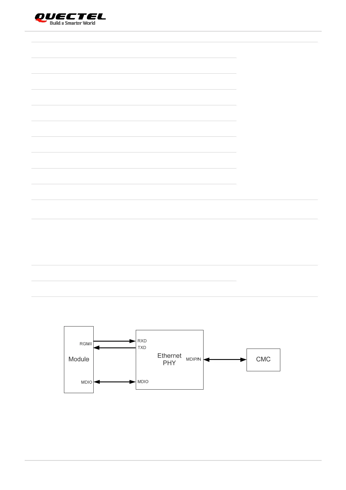
The following figure shows the simplified block diagram for Ethernet application.
Figure 27: Simplified Block Diagram for Ethernet Application
RGMII_CTL_RX 15 DI RGMII receive control
RGMII_RX_2 16 DI RGMII receive data bit 2
RGMII_RX_3 17 DI RGMII receive data bit 3
RGMII_CK_RX 19 DI RGMII receive clock
RGMII_TX_0 20 DO RGMII transmit data bit 0
RGMII_CTL_TX 21 DO RGMII transmit control
RGMII_TX_1 22 DO RGMII transmit data bit 1
RGMII_TX_2 23 DO RGMII transmit data bit 2
RGMII_CK_TX 24 DO RGMII transmit clock
RGMII_TX_3 25 DO RGMII transmit data bit 3
RGMII_PWR_EN 27 DO
Enable external LDO to supply
power to RGMII_PWR_IN
1.8 V power domain
RGMII_PWR_IN 28 PI
Power input for internal RGMII
circuit
1.8/2.5 V
power supply input.
If RGMII interface is not
used, please connect it to
VDD_EXT.
RGMII_INT 29 DI RGMII PHY interrupt output
1.8 V power domain
RGMII_RST 31 DO Reset output for RGMII PHY
 Loading...


