Automotive Module Series
AG525R-GL QuecOpen
Hardware Design
AG525R-GL_QuecOpen_Hardware_Design 63 / 104
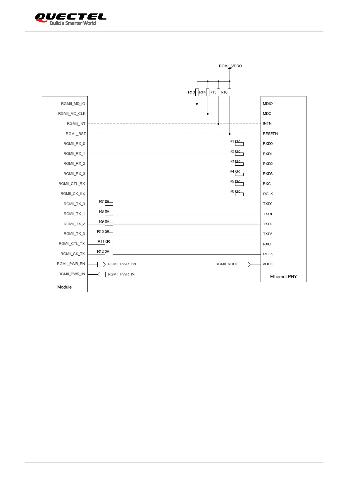
The following figure shows a reference design of RGMII interface with PHY application.
Figure 28: Reference Circuit of RGMII Interface with PHY Application
In order to enhance the reliability and availability of customers’ application, please follow the criteria below
in the Ethernet PHY circuit design:
The I/O voltage of RGMII matches with that of PHY.
The voltage of RGMII_INT and RGMII_RST matches with the I/O voltage of PHY.
The typical power consumption of RGMII_PER_IN is 300 mA @ 1.8 V.
Keep RGMII data and control signals away from RF and VBAT traces.
Assure impedance of RGMII signals trace is 50 Ω ±20%.
The length difference among CK_TX, CTL_TX and TX_[0-3] is less than 2 mm.
The length difference among CK_RX, CTL_RX and RX_[0-3] is less than 2 mm.
TX bus (CK_TX to CTL_TX/TX_[0-3]) spacing or RX bus (CK_RX to CTL_RX/RX_[0-3]) spacing is
larger than two times of the line width.
Spacing between TX bus and RX bus is larger than 2.5 times of line width.
 Loading...


