EasyManua.ls Logo

Quectel RM500Q-AE - Page 44

Quectel RM500Q-AE
87 pages
To Next Page IconTo Next Page
To Previous Page IconTo Previous Page
Loading...
5G Module Series
RM500Q-AE&RM502Q-AE Hardware Design
RM500Q-AE&RM502Q-AE_Hardware_Design 44 / 83
PCM_CLK
PCM_SYNC
PCM_DOUT
MSB
LSB
PCM_DIN
125 μs
MSB
1 2 3231
LSB
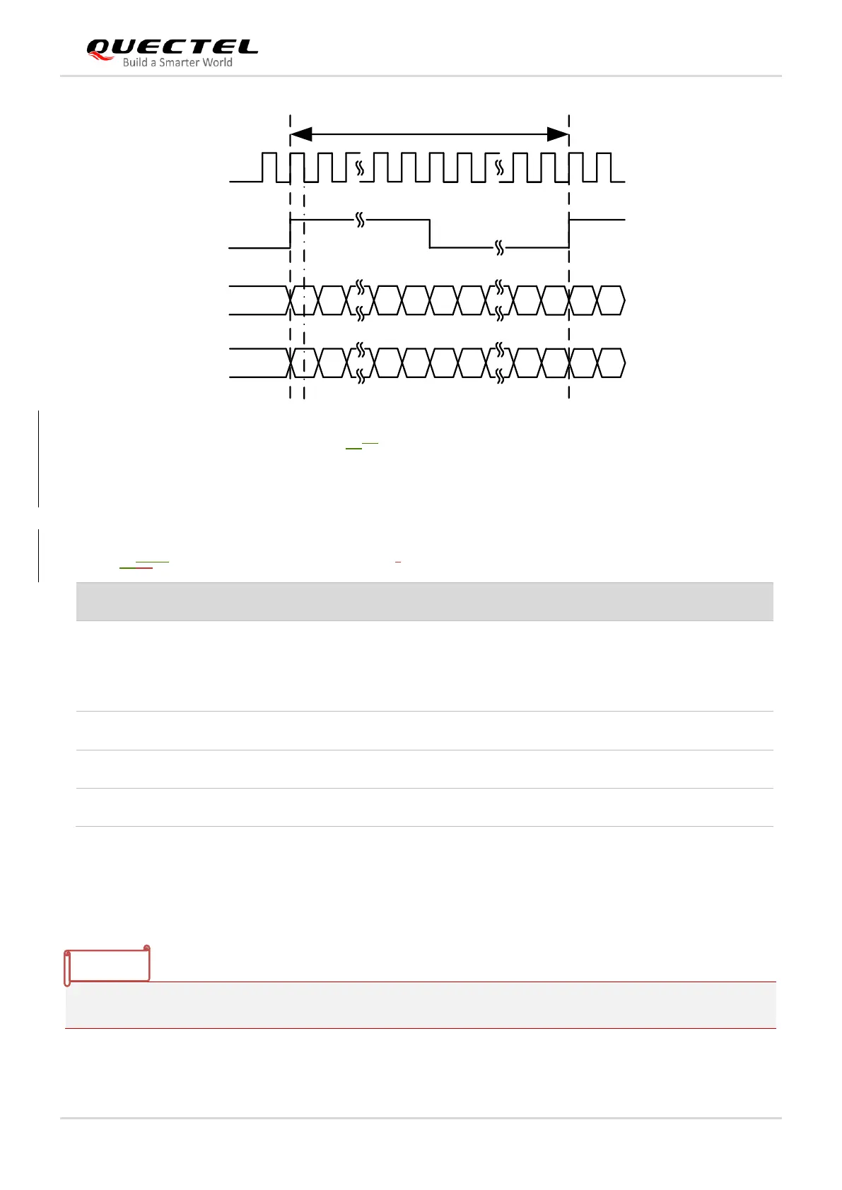
Figure 2122: Auxiliary Mode Timing
The following table shows the pin definition of PCM interface which can be applied to audio codec design.
Table 121211: Pin Definition of PCM Interface*
The clock and mode can be configured by AT command, and the default configuration is master mode
using short frame synchronization format with 2048 kHz PCM_CLK and 8 kHz PCM_SYNC. See
document [2] for details about AT+QDAI command.
“*” means under development.
Pin No.
Pin Name
I/O
Description
Comment
20
PCM_CLK
IO
PCM data bit clock
1.8 V power domain
In master mode, it is an output signal.
In slave mode, it is an input signal.
If unused, keep it open.
22
PCM_DIN
DI
PCM data input
1.8 V power domain
24
PCM_DOUT
DO
PCM data output
1.8 V power domain
28
PCM_SYNC
IO
PCM data frame sync
1.8 V power domain
NOTE

Table of Contents

Related product manuals