5G Module Series
RM500Q-GL Hardware Design
RM500Q-GL_Hardware_Design 30 / 85
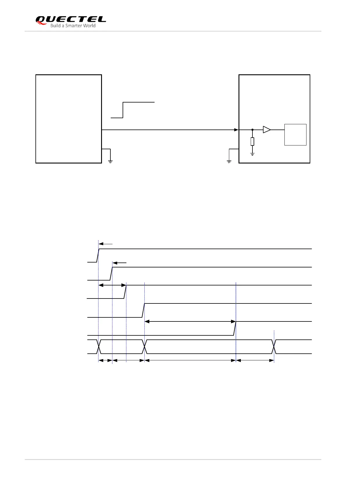
It is recommended to use a host GPIO to control FULL_CARD_POWER_OFF#. A simple reference circuit
is illustrated by the following figure.
Host Module
FULL_CARD_POWER_OFF#
PMU
GPIO
6
1.8 V or 3.3 V
R1
100k
NOTE:
The voltage of pin 6 should be no less than 1.19 V when it is at high level.
Figure 8: Turn on the Module with a Host GPIO
The timing of turn-on scenario is illustrated by the following figure.
VCC
FCPO#
20 s
Module power-on or insertion detection
USIM_VDD
Module Status
RESET#
RFFE_VIO_1V8
System turn-on and booting
V
IH
≥ 1.19 V
1.8 V or 3.0 V
System bootingInactive Active
T
power-on
T
turn-on
T
booting
T
registering
1.8 V
3.7 V
1.8 V
T
VCC-RST#
NOTE:
The host only needs to control FCPO#.
Figure 9: Turn-on Timing of the Module