EasyManua.ls Logo

Quectel RM500Q-GL

Quectel RM500Q-GL
86 pages
To Next Page IconTo Next Page
To Previous Page IconTo Previous Page
Loading...
5G Module Series
RM500Q-GL Hardware Design
RM500Q-GL_Hardware_Design 48 / 85
PCM_CLK
PCM_SYNC
PCM_DOUT
MSB
LSB
PCM_DIN
125 μs
MSB
1 2 3231
LSB
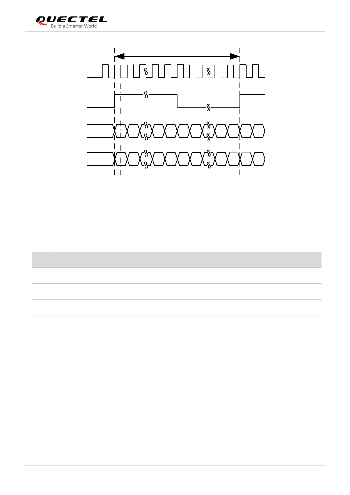
Figure 23: Auxiliary Mode Timing
The following table shows the pin definition of PCM interface which can be applied to audio codec design.
Table 19: Pin Definition of PCM Interface
The clock and mode can be configured by AT command, and the default configuration is slave mode
using short frame synchronization format with 2048 kHz PCM_CLK and 8 kHz PCM_SYNC. See
document [4] for details about AT+QDAI command.
Pin No.
Pin Name
I/O
Description
DC Characteristic
20
PCM_CLK
DIO, PD
PCM data bit clock
1.8 V
22
PCM_DIN
DI, PD
PCM data input
1.8 V
24
PCM_DOUT
DO, PD
PCM data output
1.8 V
28
PCM_SYNC
DIO, PD
PCM data frame sync
1.8 V

Table of Contents

Related product manuals