5G Module Series
RM520N-GL_Hardware_Design 37 / 84
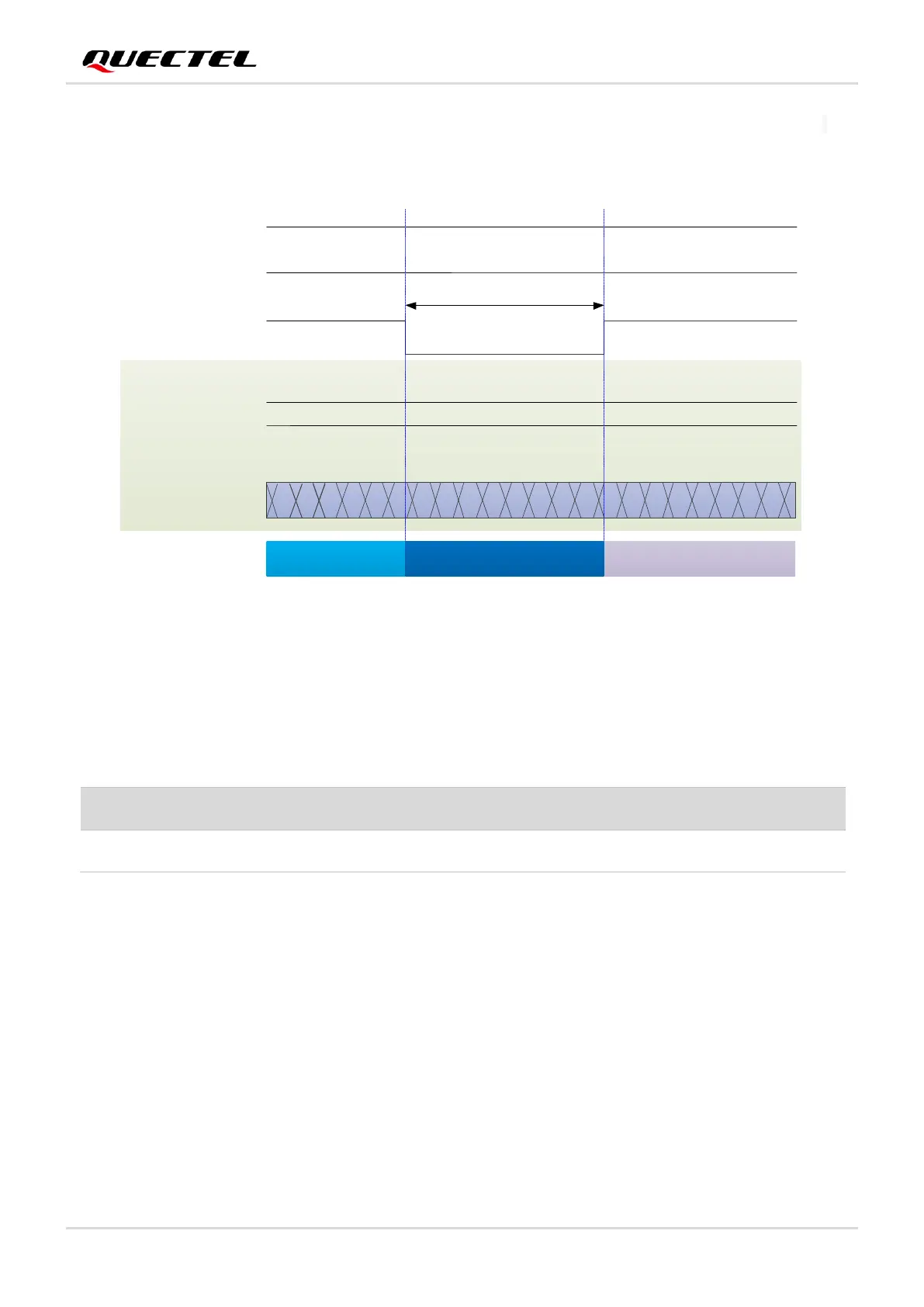
Figure below illustrates the timing of the module’s warm reset when only the reset signal is pulled low. In
this reset mode, the power of the module will not be turned off. The timing is recommended for module’s
reset with a button.
VCC(H)
FULL_CARD_
POWER_OFF#(H)
Module Status
RESET#
1.8 V
3.7 V
T
RST#
Active Booting Baseband Resetting
PCIE_CLKREQ_N
(L)
PCIE_RST_N(H)
NOTE:
When the module is in USB mode, please ignore the PCIe related signals and their timing parameters in the figure.
PCIE_REFCLK
Figure 13: Reset Timing of the Module’s Warm Reset
Table 12: Reset Timing of the Module’s Warm Reset
If your design is for the complete hardware reset of the module, then refer to the sequence diagram as
below. The following timing is recommended for module’s reset with NPN driver circuit. Sending the
command AT+CFUN=0 is necessary before reset the module.
Reset baseband chip IC only