CompactFlash Memory Card Product Manual
SanDisk CompactFlash Memory Card Product Manual © 1998 SANDISK CORPORATION 53
5.5.8 Drive/Head (LBA 27-24) Register
(Address 1F6[176]; Offset 6)
The Drive/Head register is used to select the
drive and head. It is also used to select LBA
addressing instead of cylinder/head/sector
addressing. The bits are defined as follows:
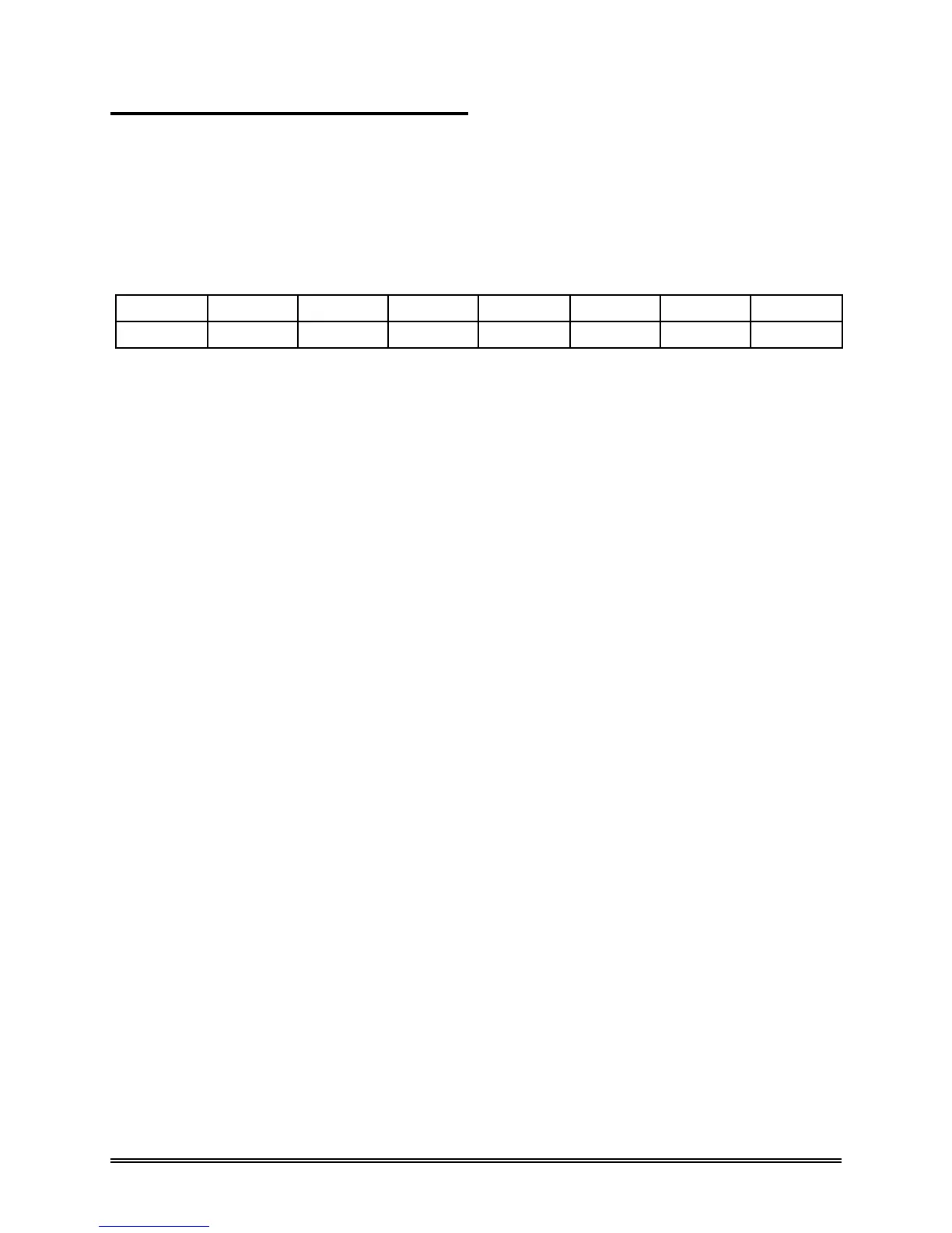
D7 D6 D5 D4 D3 D2 D1 D0
1 LBA 1 DRV HS3 HS2 HS1 HS0
Bit 7 This bit is set to 1.
Bit 6 LBA is a flag to select either Cylinder/Head/Sector (CHS) or Logical Block Address Mode (LBA).
When LBA=0, Cylinder/Head/Sector mode is selected. When LBA=1, Logical Block Address is
selected. In Logical Block Mode, the Logical Block Address is interpreted as follows:
LBA07-LBA00: Sector Number Register D7-D0.
LBA15-LBA08: Cylinder Low Register D7-D0.
LBA23-LBA16: Cylinder High Register D7-D0.
LBA27-LBA24: Drive/Head Register bits HS3-HS0.
Bit 5 This bit is set to 1.
Bit 4 (DRV) This bit will have the following meaning. DRV is the drive number. When DRV=0, drive (card) 0 is
selected When DRV=1, drive (card) 1 is selected. The CompactFlash Card is set to be Card 0 or 1
using the copy field of the PCMCIA Socket & Copy configuration register.
Bit 3 (HS3) When operating in the Cylinder , Head, Sector mode, this is bit 3 of the head number. It is Bit 27 in
the Logical Block Address mode.
Bit 2 (HS2) When operating in the Cylinder, Head, Sector mode, this is bit 2 of the head number. It is Bit 26 in
the Logical Block Address mode.
Bit 1 (HS1) When operating in the Cylinder, Head, Sector mode, this is bit 1 of the head number. It is Bit 25 in
the Logical Block Address mode.
Bit 0 (HS0) When operating in the Cylinder, Head, Sector mode, this is bit 0 of the head number. It is Bit 24 in
the Logical Block Address mode.