CompactFlash Memory Card Product Manual
SanDisk CompactFlash Memory Card Product Manual © 1998 SANDISK CORPORATION30
4.3.5 Interface/Bus Timing
There are two types of bus cycles and timing
sequences that occur in the PCMCIA type
interface, a direct mapped I/O transfer and a
memory access. The two timing sequences are
explained in detail in the PCMCIA PC Card
Standard Release 2.1. The CompactFlash Memory
Card conforms to the timing in that reference
document.
4.3.6 Attribute Memory Read Timing
Specification
The Attribute Memory access time is defined as
300 ns. Detailed timing specifications are shown
in Table 4-3.
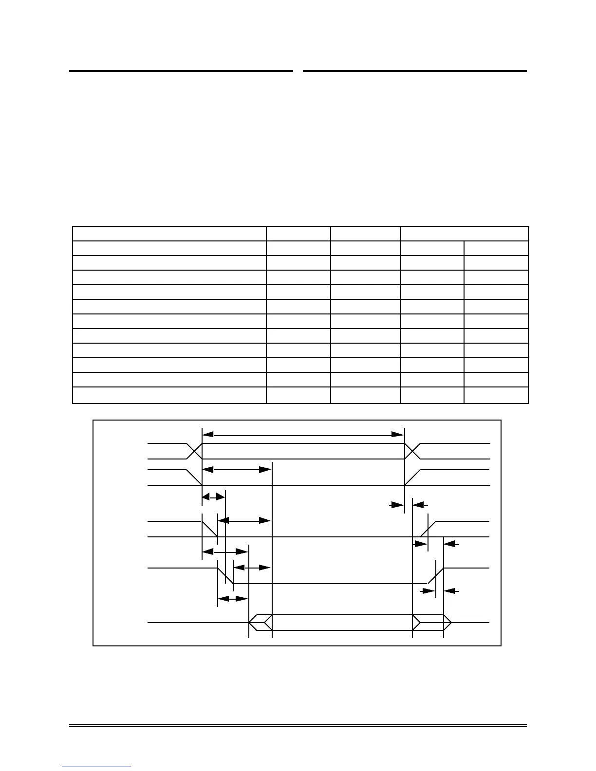
Table 4-3 Attribute Memory Read Timing
Speed Version 300 ns
Item Symbol IEEE Symbol Min ns. Max ns.
Read Cycle Time tc(R) tAVAV 300
Address Access Time ta(A) tAVQV 300
Card Enable Access Time ta(CE) tELQV 300
Output Enable Access Time ta(OE) tGLQV 150
Output Disable Time from CE tdis(CE) tEHQZ 100
Output Disable Time from OE tdis(OE) tGHQZ 100
Address Setup Time tsu (A) tAVWL 30
Output Enable Time from CE ten(CE) tELQNZ 5
Output Enable Time from OE ten(OE) tGLQNZ 5
Data Valid from Address Change tv(A) tAXQX 0
An
-CE
-OE
Dout
tc(R)
ta(A)
ta(CE)
ta(OE)
ten(OE)
ten(CE)
tv(A)
tdis(CE)
tdis(OE)
-REG
tsu(A)
Figure 4-1 Attribute Memory Read Timing Diagram
Notes: All times are in nanoseconds. Dout signifies data provided by the CompactFlash Memory Card to the
system. The -CE signal or both the -OE signal and the -WE signal must be de-asserted between consecutive
cycle operations.