CDB620-001
PNP sensor 3
V
S
GND
12 SGND
6 Shield
11
U
IN
*
A
Out
U
IN
*
GND
S3
Trigger sensor 1
ON
OFF
S3 : SGND-GND
V
S ext
Shield
U
IN
*
CDB620-001
12 SGND
6 Shield
11
U
IN
*
A
GND
S3
ON
OFF
S3 : SGND-GND
Shield
1
V
S ext
GND
A
12
2
Sens B
Sens B
2
2
4
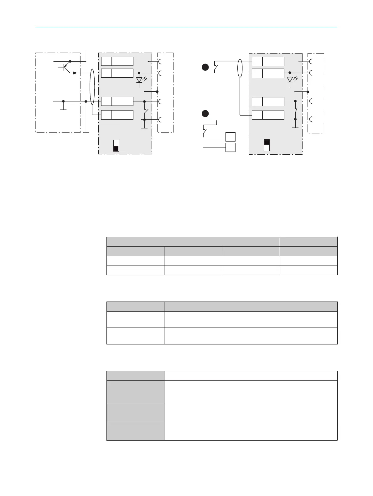
Figure 68: Left: Trigger sensor connected potential-free and supplied with power externally. Right: Alternatively switch,
!
sup‐
plied with power by connection module CDB620-001 or
"
connected potential-free and supplied with power externally. Switch
setting S3 then as in left figure.
1
Trigger sensor, e.g. for read cycle generation
2
External supply voltage V
S ext
3
PNP sensor
4
Supply voltage V
S
Table 57: Assignment of placeholders to the digital inputs
CDB620-001 Device
Terminal A Signal B Pin C Sensor D
10 Sens 1 14 1
13 Sens 2 4 2
Function of switch S3
Table 58: Switch S3: SGND - GND
Switch setting Function
ON GND of the trigger sensor connected with GND of CDB620-001 and
GND of the device
OFF Trigger sensor connected potential-free at CDB620-001 and device.
Common, isolated reference potential of all digital inputs is SGND.
Characteristic data of the digital inputs
Table 59: Characteristic data of the digital inputs “Sensor 1” and “Sensor 2”
Type Switching
Switching behavior Power to the input starts the assigned function, e.g. start read cycle.
Default setting in the device: logic not inverted (active high), debounce
time 10 ms
Properties
•
Opto-decoupled, reverse polarity protected
•
Can be wired with PNP output of a trigger sensor
Electrical values Low: V
in
1)
≤ 2 V; I
in
2)
≤ 0.3 mA
High: 6 V ≤ V
in
≤ 30 V; 0.7 mA ≤ I
in
≤ 5 mA
1)
Input Voltage
2)
Input current
ANNEX 13
8022502/15NT/2020-02-11 | SICK O P E R A T I N G I N S T R U C T I O N S | Lector621
111
Subject to change without notice