SIM5300E_Hardware_Design_V1.02
C101
59
MODULE
60
RF_ANT
GND
C102
61
GND
R101
Antenna feed pad
Matching circuit
RF test connector
J101
TVS
R102
D101
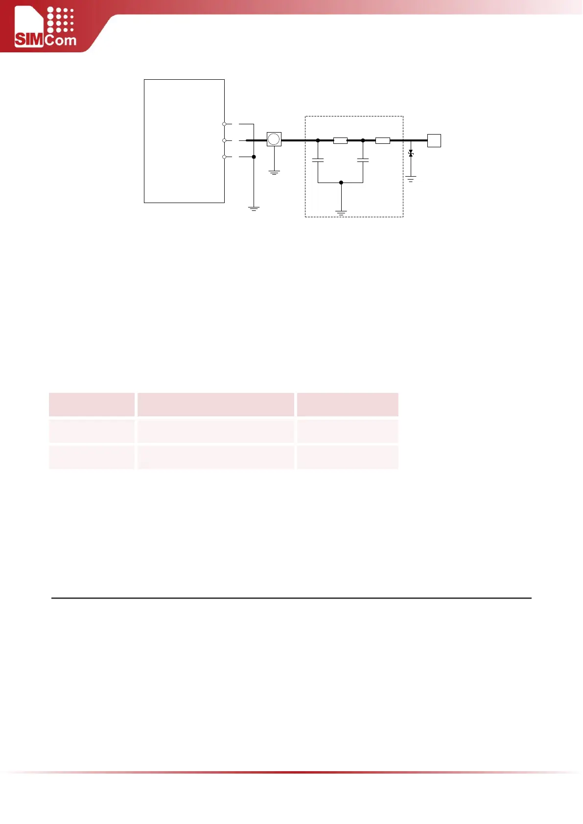
Figure 38: Antenna matching circuit
In this figure, the components R101, R102, C101 and C102 is used for antenna matching, the components’
value can only be got after the antenna tuning. Usually, matching components’ value is provided by antenna
vendor, and the default value of R101 and R102are 0Ω .Reserve the place of C101 and C102, they are used
for tuning. The component D101 is a bidirectional TVS component, which is used for ESD protection. The
recommended part numbers of the TVS are listed in the following table:
Table 19: TVS part number list
The RF test connector in figure 37 shown above is used for conducted RF performance test, and should be
placed as close as possible to the module’s RF_ANT pin. The traces in bold type should be 50Ω impedance
controlled line in PCB layout.
5 ELECTRICAL, RELIABILITY AND RADIO CHARACTERISTICS
5.1 ABSOLUTE MAXIMUM RATINGS
The absolute maximum ratings stated in following table are stress ratings under non-operating conditions.
Stresses beyond any of these limits will cause permanent damage to SIM5300E.