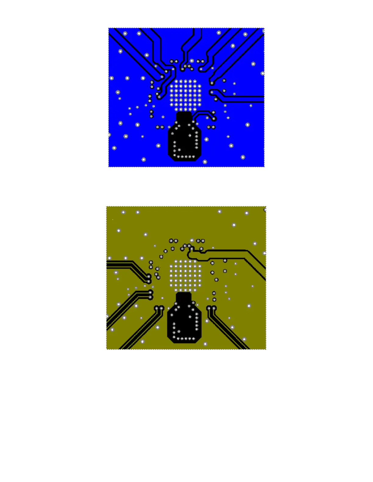
Figure 11.12. Power Plane and Clock Output Power Supply Traces (Layer 4)
The following figure shows layer 5 and the clock input traces. Similar to the clock output traces, they are routed to an inner layer and
surrounded by ground to avoid crosstalk.
Figure 11.13. Clock Input Traces (Layer 5)
The following figure shows the bottom layer, which continues the void underneath the shield. Layer 6 and layer 1 are mainly used for
low speed CMOS control and status signals for which crosstalk is not a significant issue. PCB ground can be placed under the X1X2
shield as long as the PCB ground is at least 0.05 inches below it.
Si5341, Si5340 Rev D Family Reference Manual • Crystal and Device Circuit Layout Recommendations
Skyworks Solutions, Inc. • Phone [781] 376-3000 • Fax [781] 376-3100 • sales@skyworksinc.com • www.skyworksinc.com
54 Rev. 1.3 • Skyworks Proprietary Information • Products and Product Information are Subject to Change Without Notice • July 26, 2021 54
 Loading...