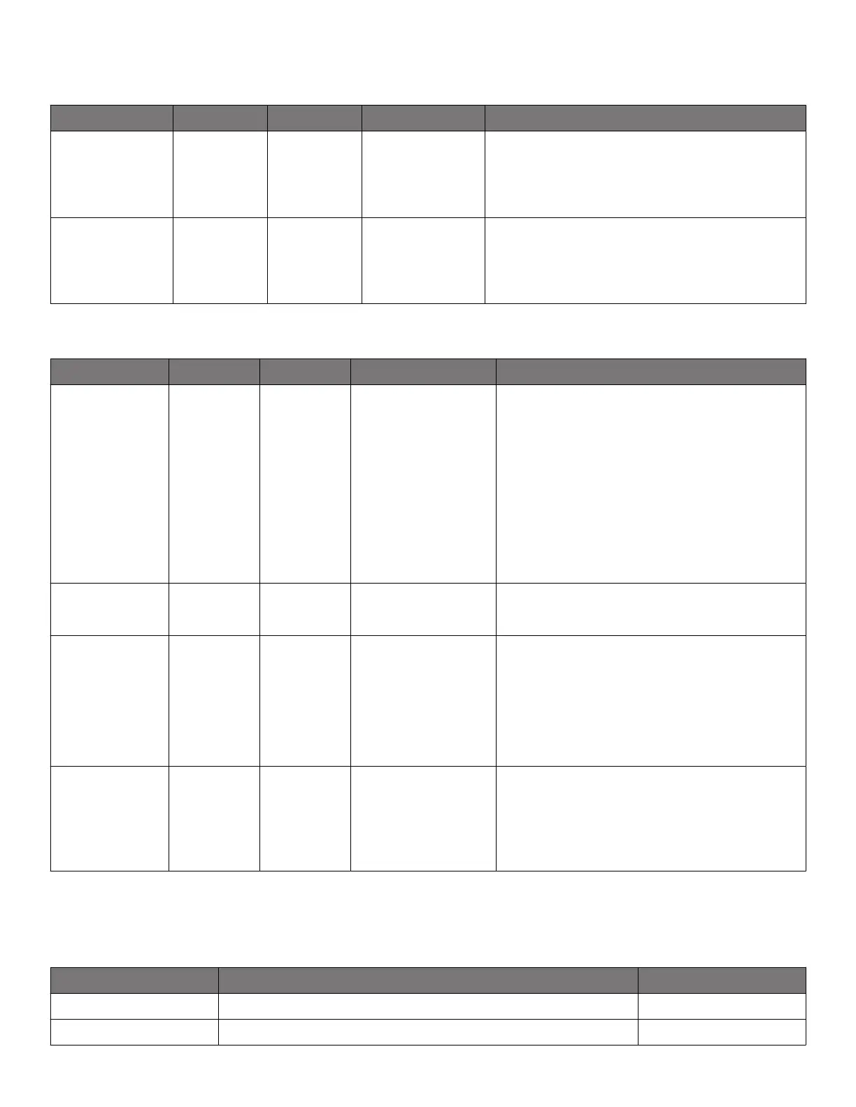
Table 14.134. 0x0114 Output 0 Amplitude and Common Mode Voltage
Reg Address Bit Field Type Setting Name Description
0x0114 3:0 R/W OUT0_CM This field only applies when OUT0_FORMAT=1 or 2.
See Table 5.4 Settings for LVDS, LVPECL, and HCSL
on page 25 and 15. Appendix—Setting the Differential
Output Driver to Non-Standard Amplitudes for details of
the settings.
0x0114 6:4 R/W OUT0_AMPL This field only applies when OUT0_FORMAT=1, 2, or 3.
See Table 5.4 Settings for LVDS, LVPECL, and HCSL
on page 25 and 15. Appendix—Setting the Differential
Output Driver to Non-Standard Amplitudes for details of
the settings when the OUT0_FORMAT=1 or 2.
Table 14.135. 0x0115 Clock Output 0 Mux and Inversion
Reg Address Bit Field Type Setting Name Description
0x0115 2:0 R/W OUT0_MUX_SEL
Output driver 0 input mux select.This selects the
source of the multisynth.
0: N0
1: N1
2: N2
3: N3
4: Reserved
5-7: Reserved
0x0115 3 R/W OUT0_VDD_SEL_EN Output Driver VDD Select Enable. Set to 1
for normal operation.
0x0115 5:4 R/W OUT0_VDD_SEL Output Driver VDD Select
0: 3.3V
1: 1.8V
2: 2.5V
3: Reserved
0x0115 7:6 R/W OUT0_INV CLK and CLKb not inverted
CLKb inverted
CLK and CLKb inverted
CLK inverted
Each of the 4 output drivers can be connected to any of the N dividers. More than 1 output driver can connect to the same N divider.
The four output drivers are all identical. The single set of descriptions above for output driver 0 applies to the other three output drivers.
Table 14.136. Registers for OUT1,2,3 as per OUT0 Above
Register Address Description (Same as) Address
0x0117 OUT1_PDN, OUT1_OE, OUT1_RDIV_FORCE2 0x0112
0x0118 OUT1_FORMAT, _SYNC_EN, DIS_STATE, _CMOS_DRV 0x0113
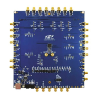
Si5341, Si5340 Rev D Family Reference Manual • Register Map
Skyworks Solutions, Inc. • Phone [781] 376-3000 • Fax [781] 376-3100 • sales@skyworksinc.com • www.skyworksinc.com
95 Rev. 1.3 • Skyworks Proprietary Information • Products and Product Information are Subject to Change Without Notice • July 26, 2021 95