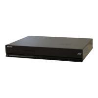
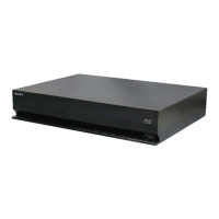
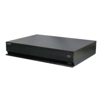
HBD-E2100/E3100/E3200/E4100/E6100
4
1. SERVICING NOTES .............................................. 5
2. DISASSEMBLY
2-1. Disassembly Flow ........................................................... 13
2-2. How To Bend FFC .......................................................... 14
2-3. Case ................................................................................. 15
2-4. Panel Loading Assy ........................................................ 15
2-5. Front Panel Assy ............................................................. 16
2-6. BD Drive (BPX-7) .......................................................... 16
2-7. POWER KEY Board, WLAN/BT COMBO Card,
KARAOKE Board (SP, RU), PANEL Board .................. 17
2-8. MB1002 Board ............................................................... 18
2-9. AMP Board ..................................................................... 18
2-10. SWITCHING REGULATOR (SWR1) ........................... 19
2-11. Optical Pick-up Block (KEM480AAA),
Wire (Flat Type) .............................................................. 20
3. TEST MODE ............................................................. 21
4. ELECTRICAL CHECK .......................................... 32
5. TROUBLESHOOTING ........................................... 33
6. DIAGRAMS
6-1. Block Diagram - SERVO Section - ................................ 37
6-2. Block Diagram - MEMORY/HDMI Section - ................ 38
6-3. Block Diagram - MAIN Section - ................................... 39
6-4. Block Diagram - AMP Section - ..................................... 40
6-5. Block Diagram - POWER SUPPLY Section - ................ 41
6-6. Printed Wiring Board
- MB1002 Board (Component Side) - ............................ 43
6-7. Printed Wiring Board
- MB1002 Board (Conductor Side) - .............................. 44
6-8. Schematic Diagram - MB1002 Board (1/6) - ................. 45
6-9. Schematic Diagram - MB1002 Board (2/6) - ................. 46
6-10. Schematic Diagram - MB1002 Board (3/6) - ................. 47
6-11. Schematic Diagram - MB1002 Board (4/6) - ................. 48
6-12. Schematic Diagram - MB1002 Board (5/6) - ................. 49
6-13. Schematic Diagram - MB1002 Board (6/6) - ................. 50
6-14. Printed Wiring Board
- AMP Board (Component Side) - .................................. 51
6-15. Printed Wiring Board
- AMP Board (Conductor Side) - .................................... 52
6-16. Schematic Diagram - AMP Board (1/3) - ....................... 53
6-17. Schematic Diagram - AMP Board (2/3) - ....................... 54
6-18. Schematic Diagram - AMP Board (3/3) - ....................... 55
TABLE OF CONTENTS
6-19. Printed Wiring Board - PANEL Board - ......................... 56
6-20. Schematic Diagram - PANEL Board - ............................ 57
6-21. Printed Wiring Board
- KARAOKE Board (SP, RU) - ...................................... 58
6-22. Schematic Diagram
- KARAOKE Board (SP, RU) - ...................................... 58
6-23. Printed Wiring Board - POWER KEY Board -............... 58
6-24. Schematic Diagram - POWER KEY Board - ................. 58
7. EXPLODED VIEWS
7-1. Case Section .................................................................... 76
7-2. Front Panel Section ......................................................... 77
7-3. Chassis Bottom Section .................................................. 78
7-4. Chassis Section ............................................................... 80
7-5. BD Drive Section (BPX-7) ............................................. 81
8. ELECTRICAL PARTS LIST .............................. 82
NOTES ON CHIP COMPONENT REPLACEMENT
• Never reuse a disconnected chip component.
• Notice that the minus side of a tantalum capacitor may be dam-
aged by heat.
FLEXIBLE CIRCUIT BOARD REPAIRING
• Keep the temperature of soldering iron around 270 °C during
repairing.
• Do not touch the soldering iron on the same conductor of the
circuit board (within 3 times).
• Be careful not to apply force on the conductor when soldering
or unsoldering.
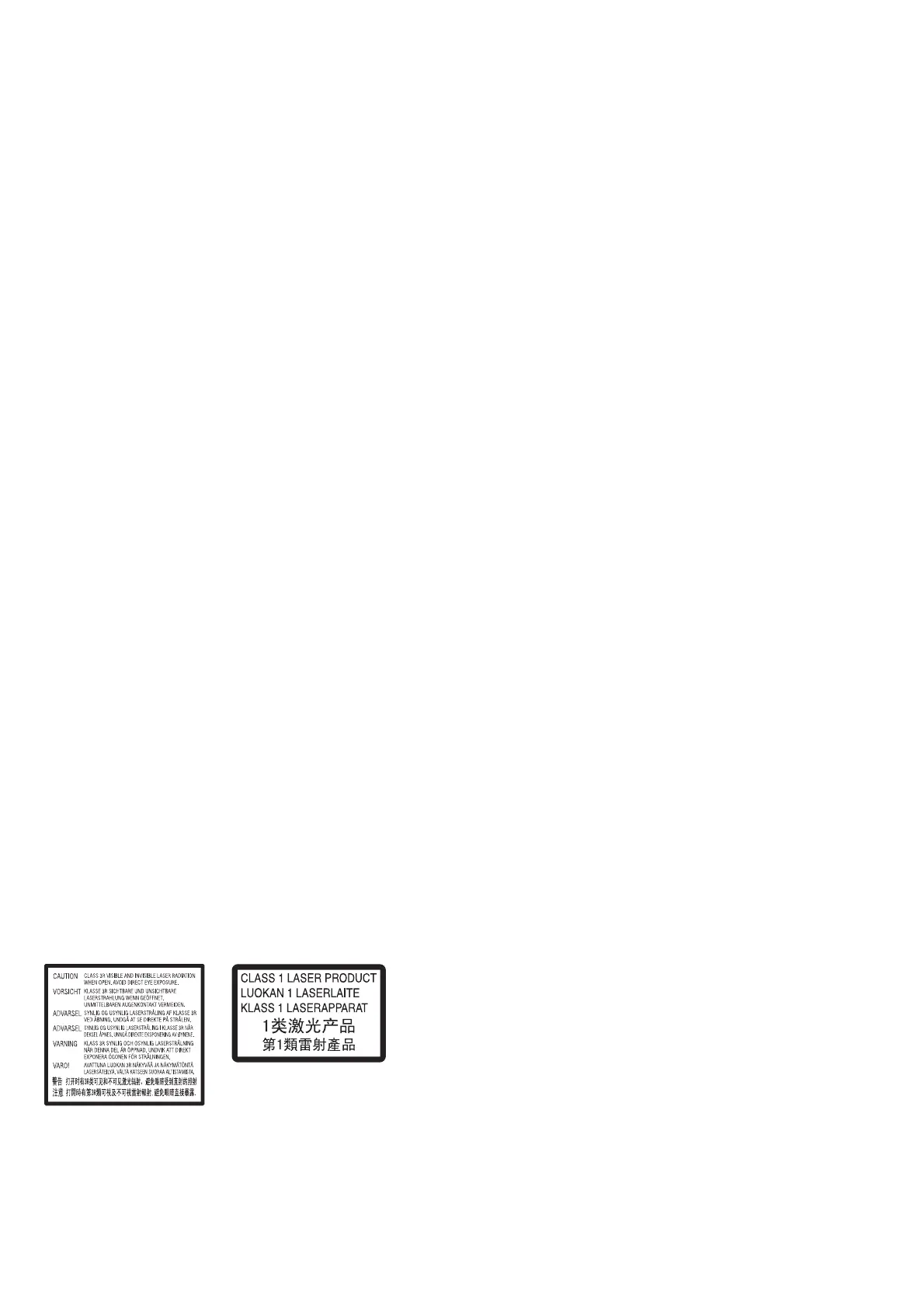
This appliance is classified as a
CLASS 3R LASER product.
Visible and invisible laser radiation
is emitted when the laser protective
housing is opened, so be sure to
avoid direct eye exposure.
This appliance is classified as a
CLASS 1 LASER product. This
marking is located on the rear
exterior.
The nameplate is located on the
bottom exterior.
This marking is located on the laser
protective housing inside the
enclosure.
Ver. 1.5