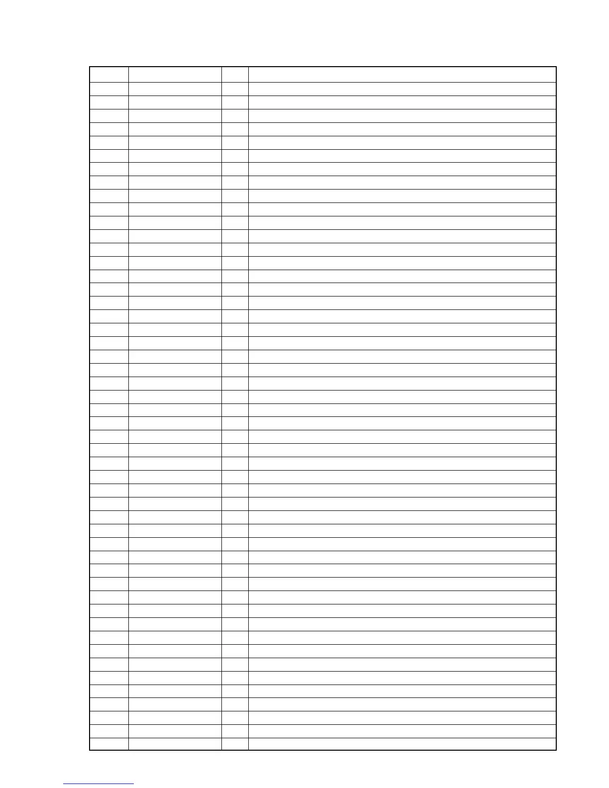
59
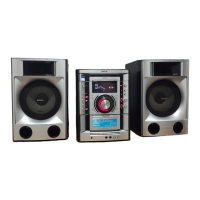
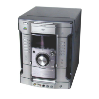
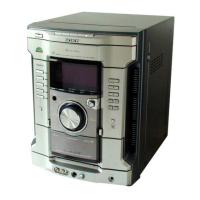
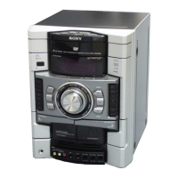
HCD-GNX780/GNX880
Pin No. Pin Name I/O Description
49 AVSS3 – Ground terminal
50 CLTV I Multiplier VCO1 control voltage input
51 FILO O Master PLL (slave = digital PLL) filter signal output
52 FILI I Master PLL filter signal input
53 PCO O Master PLL charge pump signal output
54 AVDD5 – Power supply terminal (+3.3V)
55 DDVROUT O DC/DC converter output (+2.5V)
56 DDVRSEN I DC/DC converter output voltage monitor signal input
57 AVSS5 – Ground terminal
58 DDCR I DC/DC converter reset signal input
59 NC – Not used (Open)
60 BCKI I D/A interface bit clock input
61 PCMDI I D/A interface serial data input
62 LRCKl I D/A interface LR clock input
63 LRCK O D/A interface LR clock output f = Fs
64 VSS – Ground terminal
65 PCMD O D/A interface serial data output
66 BCK O D/A interface bit clock output
67 VDD – Power supply terminal (+2.5V)
68 EMPH O High when the playback disc has emphasis, low it has not
69 EMPHI I High when de-emphasis is ON, low when input OFF
70 IOVDD2 – Power supply terminal (+3.3V)
71 DOUT O Digital Out signal output
72 TEST I Test terminal (Connected to ground)
73 TEST1 I Test terminal (Connected to ground)
74 IOVSS2 – Ground terminal
75 NC – Not used (Open)
76 XVSS – Ground terminal
77 XTAO O Crystal oscillation circuit signal output
78 XTAI I Crystal oscillation circuit signal input
79 XVDD – Power supply terminal (+2.5V)
80 AVDD1 – Power supply terminal (+3.3V)
81 AOUT1 O L-ch analog signal output
82 VREFL O L-ch reference voltage output
83 AVSS1 – Ground terminal
84 AVSS2 – Ground terminal
85 VREFR O R-ch reference voltage output
86 AOUT2 O R-ch analog signal output
87 AVDD2 – Power supply terminal (+3.3V)
88 NC – Not used (Open)
89 IOVDD0 – Power supply terminal (+3.3V)
90 RMUT O Not used (Open)
91 LMUT O Not used (Open)
92 NC – Not used (Open)
93 XTSL I Crystal selection signal input (Pull down)
94 IOVSS0 – Ground terminal
95 XTACN I Oscillation circuit control signal input (“H”: self-oscillation, “L”: oscillation stop)
96 SQSO O Not used (Open)
97 SQCK I SQSO readout clock input (Connected to +VDD(+3.3V))
98 SBSO O Sub code P to W serial signal output