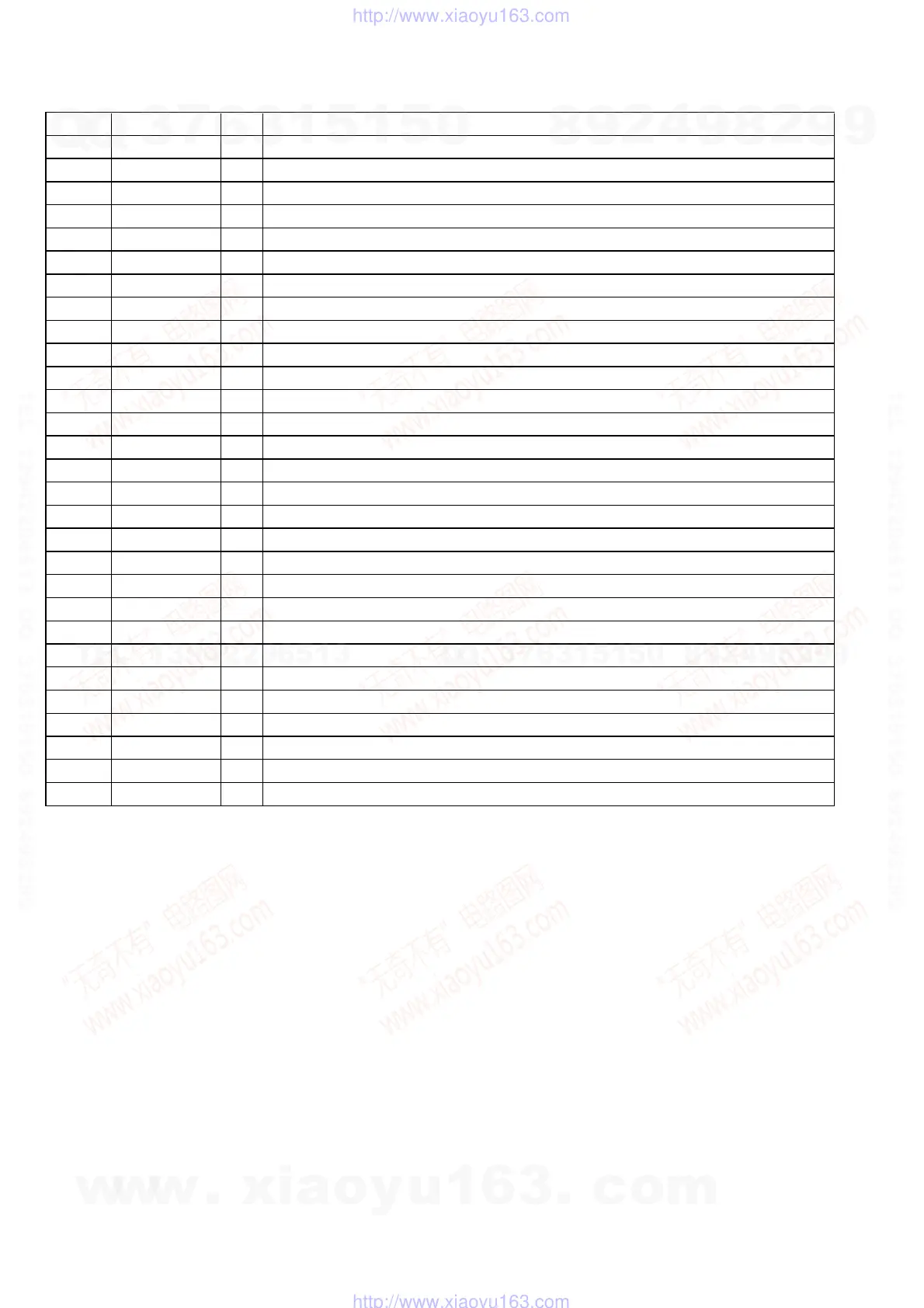
46
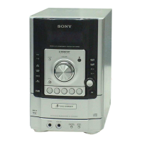
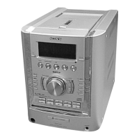
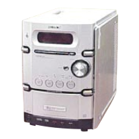
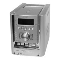
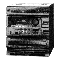
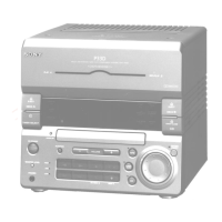
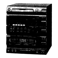
HCD-HPR90/HPR99XM
Pin No.
Pin Name I/O Description
92
SVDD - Power supply terminal (+2.5V)
93
JTAGTCK I Clock signal input terminal (for JTAG) Not used
94
JTAGTDI I Data input terminal (for JTAG) Not used
95
JTAGTDO O Data output terminal (for JTAG) Not used
96
JTAGTMS I Mode select signal input terminal (for JTAG) Not used
97
TRST I Reset signal input terminal (for JTAG) Not used
98
VSS - Ground terminal
99
VDD - Power supply terminal (+1.8V)
100
IOVDD2 - Power supply terminal (+3.3V)
101 DOUT O
Digital audio signal output terminal Not used
102 TEST I
Input terminal for the test Normally: fixed at "L"
103 TES1 I
Input terminal for the test Normally: fixed at "L"
104
IOVSS2 - Ground terminal
105
PLLVDD - Power supply terminal (+1.8V)
106
PLLVSS - Ground terminal
107
XVSS - Ground terminal
108
XTAO O System clock output terminal (16.9344 MHz)
109
XTAI I System clock input terminal (16.9344 MHz)
110
XVDD - Power supply terminal (+1.8V)
111
AVDD1 - Power supply terminal (+3.3V)
112
AOUT1 O L-ch analog audio signal output terminal
113
VREFL O L-ch reference voltage output terminal
114
AVSS1 - Ground terminal
115
AVSS2 - Ground terminal
116
VREFR O R-ch reference voltage output terminal
117
AOUT2 O R-ch analog audio signal output terminal
118
AVDD2 - Power supply terminal (+3.3V)
119
IOVDD0 - Power supply terminal (+3.3V)
120
IOVSS0 - Ground terminal
w
w
w
.
x
i
a
o
y
u
1
6
3
.
c
o
m
Q
Q
3
7
6
3
1
5
1
5
0
9
9
2
8
9
4
2
9
8
T
E
L
1
3
9
4
2
2
9
6
5
1
3
9
9
2
8
9
4
2
9
8
0
5
1
5
1
3
6
7
3
Q
Q
TEL 13942296513 QQ 376315150 892498299
TEL 13942296513 QQ 376315150 892498299
http://www.xiaoyu163.com
http://www.xiaoyu163.com