35
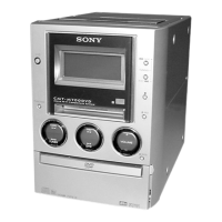
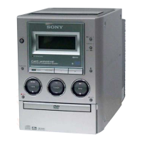
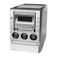
HCD-M70
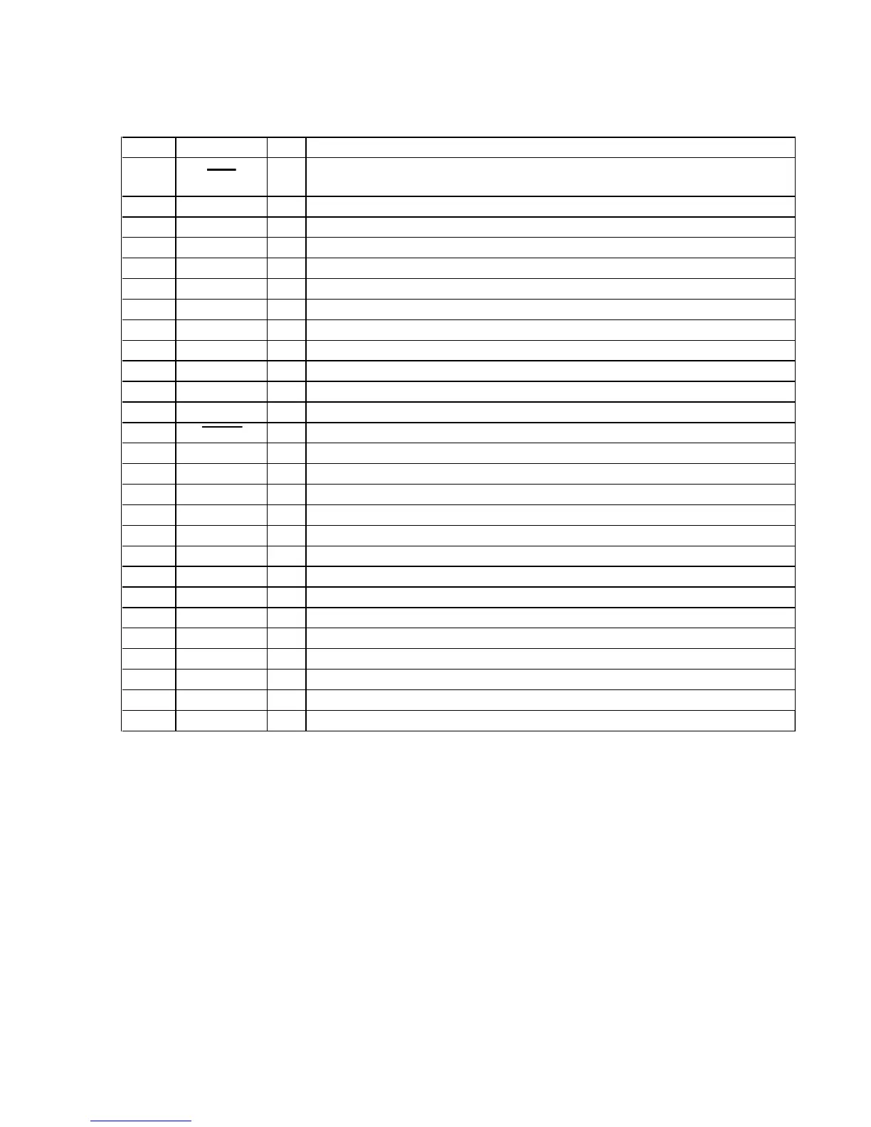
Pin No. Pin Name I/O Description
38
RST I
System reset signal input “L”: reset
For several hundreds msec. after the power supply rises, “L”: is input, then it changes to “H”
39 EXTAL1
IMain system clock input terminal (4.19MHz)
40
XTAL1 O Main system clock output terminal (4.19MHz)
41
VSS — Ground terminal
42
XTAL2 O System clock output terminal Not used
43
EXTAL2 I System clock input terminal Not used
44
AVREF I Reference voltage (+5V) input terminal (for A/D conversion)
45
AVSS — Ground terminal (for A/D conversion)
46
VL O Liquid crystal display bias on/off control signal output
47 to 49
VLC3 to VLC1 — Power supply terminal for the liquid crystal display bias
50 to 53 COM0 to COM3
O Common drive signal output to the liquid crystal display
54 to 85
SEG0 to SEG31 O Segment drive signal output to the liquid crystal display
86
C-RST O Reset signal output to the digital signal processor and motor/coil driver “L”: reset
87
AU-CE
O
Chip enable signal output to the electrical volume
88
SDA O Serial data output to the electrical volume
89
VDD — Power supply terminal (+5V)
90
NC — Not used
91
VSS — Ground terminal
92
TX O Sub system clock output terminal (32.768kHz)
93
TEX I Sub system clock input terminal (32.768kHz)
94 TRAY-CLOSE
OMotor drive signal (close direction) output to the loading motor driver “H” active
95 TRAY-OPEN
OMotor drive signal (open direction) output to the loading motor driver “H” active
96
TC-ON O LED drive signal output of the TAPE indicator “H”: LED on
97
AU-MUTE O Audio line muting on/off control signal output “H”: muting on
98
STAND-BY LED
O LED drive signal output of the standby indicator “H”: LED on
99
WP I Wakeup control signal input
100
C-SCOR I Subcode sync (S0+S1) detection signal input from the digital signal processor