37
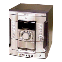
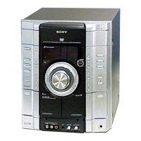
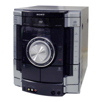
HCD-RV777D/RV888D/RV999D
Pin No. Pin Name I/O Pin Description
59, 60 HA0, HA2 I Not used in this set. (Fixed at H.)
61 VSS — Ground pin
62, 63 HCS0, HCS1 I Not used in this set. (Open)
64 VDD — Power supply pin (+3.2 V)
65 DASP I/O Not used in this set. (Fixed at H.)
66 to 69 MDB0 to MDB3 I/O Two-way data bus signal input from/output to 16Mbit D-RAM IC.
70 VSS — Ground pin
71 MDB4 I/O Two-way data bus signal input from/output to 16Mbit D-RAM IC.
72 VDD5V — Power supply pin (+5 V)
73 to 75 MDB5 to MDB7 I/O Two-way data bus signal input from/output to 16Mbit D-RAM IC.
76 XMWR O Write enable signal output to 16Mbit D-RAM IC.
77 VDD — Power supply pin (+3.2 V)
78 XRAS O Row address strobe signal output to 16Mbit D-RAM IC.
79, 80 MA0, MA1 O Address signal output to 16Mbit D-RAM IC.
81 VSS — Ground pin
82 to 87 MA2 to MA7 O Address signal output to 16Mbit D-RAM IC.
88 VDD — Power supply pin (+3.2 V)
89 MA8 O Address signal output to 16Mbit D-RAM IC.
90 VSS — Ground pin
91 MA9/mnt0 O Address signal output to 16Mbit D-RAM IC.
92 MA10/mnt1 O EEPROM ready signal output to mechanism control IC.
93 MA11/mnt2 O Address signal output to 16Mbit D-RAM IC.
94 XMOE O Output enable signal output to 16Mbit D-RAM IC.
95 XCAS O Column address strobe signal output to 16Mbit D-RAM IC.
96, 97 MDB8, MDB9 I/O Two-way data bus signal input from/output to 16Mbit D-RAM IC.
98 VSS — Ground pin
99 MDBA I/O Two-way data bus signal input from/output to 16Mbit D-RAM IC.
100 VDD — Power supply pin (+3.2 V)
101, 102 MDBB, MDBC I/O Two-way data bus signal input from/output to 16Mbit D-RAM IC.
103 VDD5V — Power supply pin (+5 V)
104 to 106 MDBD to MDBF I/O Two-way data bus signal input from/output to 16Mbit D-RAM IC.
107 GFS O Guard frame sync signal output to mechanism control IC.
108 VSS — Ground pin
109 APE0 O Absolute phase error signal output
110 VDD — Power supply pin (+3.2 V)
111 DASY0 O RF binary signal output
112 GNDA5 — Ground pin
113, 114 ASF1, ASF2 O Filter connected pin for selection the constant asymmetry compensation.
115 DASY1 I Analog signal input after integrated from the RF binary signal.
116 RFDCC I Input pin for adjusting DC cut high-pass filter for RF signal.
117 RFIN I RF signal input from RS-232C. (for check)
118, 119 VCCA5, VCCA4 — Power supply pin (+3.2 V)
120 VCOR1 I VCO oscillating range setting resistor connected
121 VCOIN I VCO input
122, 123 GNDA4, GNDA3 — Ground pin
124 LPF5 O Inverted signal output to operation amplifier from PLL loop filter.
125 VC1 I Middle point voltage (+1.65 V) input
126, 127 LPF2, LPF1 I Inverted signal input from operation amplifier from PLL loop filter.
128, 129 VCCA3, VCCA2 — Power supply pin (+3.2 V)
130 PD0 O Signal output to charge pump for phase comparator.
131 PDHVCC O Middle point voltage output to RF PLL.
132 FDO O Signal output to charge pump for frequency comparator.
133, 134 GNDA2, GNDA1 — Ground pin
w
w
w
.
x
i
a
o
y
u
1
6
3
.
c
o
m
Q
Q
3
7
6
3
1
5
1
5
0
9
9
2
8
9
4
2
9
8
T
E
L
1
3
9
4
2
2
9
6
5
1
3
9
9
2
8
9
4
2
9
8
0
5
1
5
1
3
6
7
3
Q
Q
TEL 13942296513 QQ 376315150 892498299
TEL 13942296513 QQ 376315150 892498299
http://www.xiaoyu163.com
http://www.xiaoyu163.com
 Loading...