38
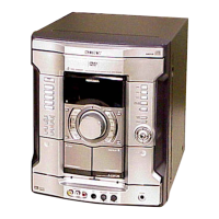
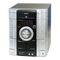
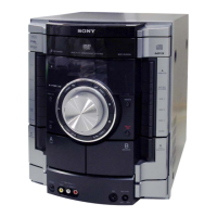
HCD-RV777D/RV888D/RV999D
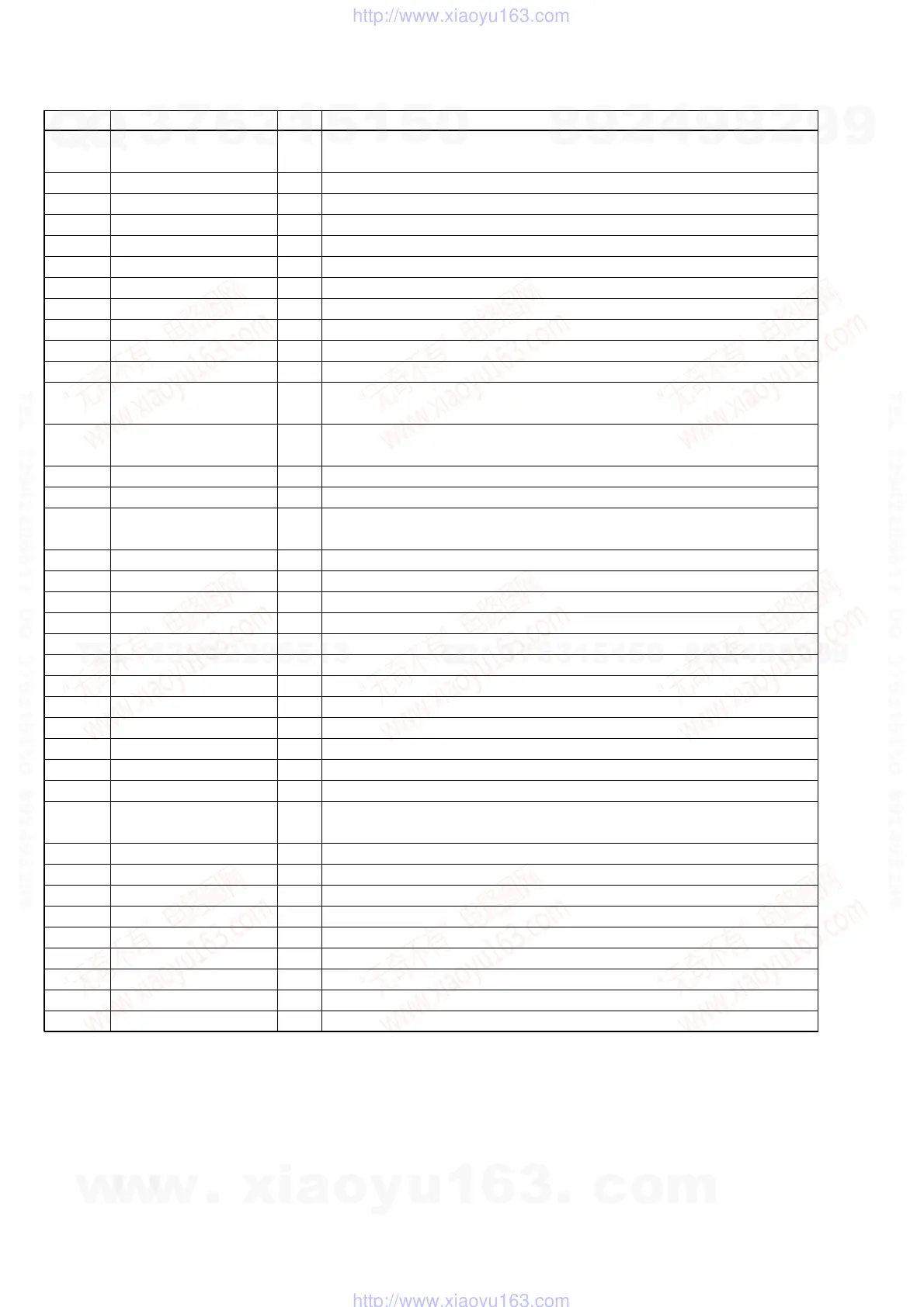
Pin No. Pin Name I/O Pin Description
135 SPO O
Spindle motor control signal output to focus/tracking coil driver, spindle/sled motor
driver IC.
136 VC2 I Middle point voltage (+1.65 V) input
137 MDIN2 I Spindle motor servo drive signal input
138 MDIN1 I MDP input
139 VCCA1 — Power supply pin (+3.2 V)
140 CLVS O Control signal output to selection the spindle control filter constant at CLVS.
141 VSS — Ground pin
142 MDSOUT O Frequency error output pin of internal CLV circuit.
143 VDD — Power supply pin (+3.2 V)
144 MDPOUT O Phase error output pin of internal CLV circuit.
145 DFCT I DFCT signal input
146 GSCOR I
Guard subcode sync (S0+S1) detection signal input from CD decoder, digital servo
processor IC.
147 EXCK O
Subcode serial data reading clock signal output to CD decoder, digital servo processor
IC.
148 SBIN I Subcode serial data input from CD decoder, digital servo processor IC.
149 VSS — Ground pin
150 SCOR I
Subcode sync (S0+S1) detection signal input from CD decoder, digital servo
processor IC.
151 WFCK I Write frame clock signal input from CD decoder, digital servo processor IC.
152 VDD5V — Power supply pin (+5 V)
153 XRCI I Not used in this set. (Fixed at L.)
154 VDDS — Power supply pin (+5 V)
155 C2PO I C2 pointer signal input from CD decoder, digital servo processor IC.
156 VDD — Power supply pin (+3.2 V)
157 DBCK O Not used in this set. (Open)
158 BCLK I Bit clock signal (2.8224 MHz) input from CD decoder, digital servo processor IC.
159 DDAT O Not used in this set. (Open)
160 MDAT I Signal data input from CD decoder, digital servo processor IC.
161 VSS — Ground pin
162 DLRC O Not used in this set. (Open)
163 LRCK I
L/R sampling clock signal (44.1 kHz) input from CD decoder, digital servo processor
IC.
164 XRST I Reset signal input from mechanism control IC. (L: reset)
165 IFS0 I Not used in this set. (Fixed at L.)
166 IFS1 I Not used in this set. (Fixed at H.)
167 XTAL I 33.8688 MHz clock signal input from clock generator IC.
168 VSS — Ground pin
169 XTL2 O 33.8688 MHz clock signal output to clock generator IC.
170 XTL1 I 33.8688 MHz clock signal input from clock generator IC.
171 VDD — Power supply pin (+3.2 V)
172 to 176 D0 to D4 I/O Two-way data bus signal input from/output to mechanism control IC.
w
w
w
.
x
i
a
o
y
u
1
6
3
.
c
o
m
Q
Q
3
7
6
3
1
5
1
5
0
9
9
2
8
9
4
2
9
8
T
E
L
1
3
9
4
2
2
9
6
5
1
3
9
9
2
8
9
4
2
9
8
0
5
1
5
1
3
6
7
3
Q
Q
TEL 13942296513 QQ 376315150 892498299
TEL 13942296513 QQ 376315150 892498299
http://www.xiaoyu163.com
http://www.xiaoyu163.com
 Loading...