46
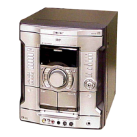
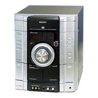
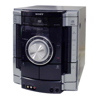
HCD-RV777D/RV888D/RV999D
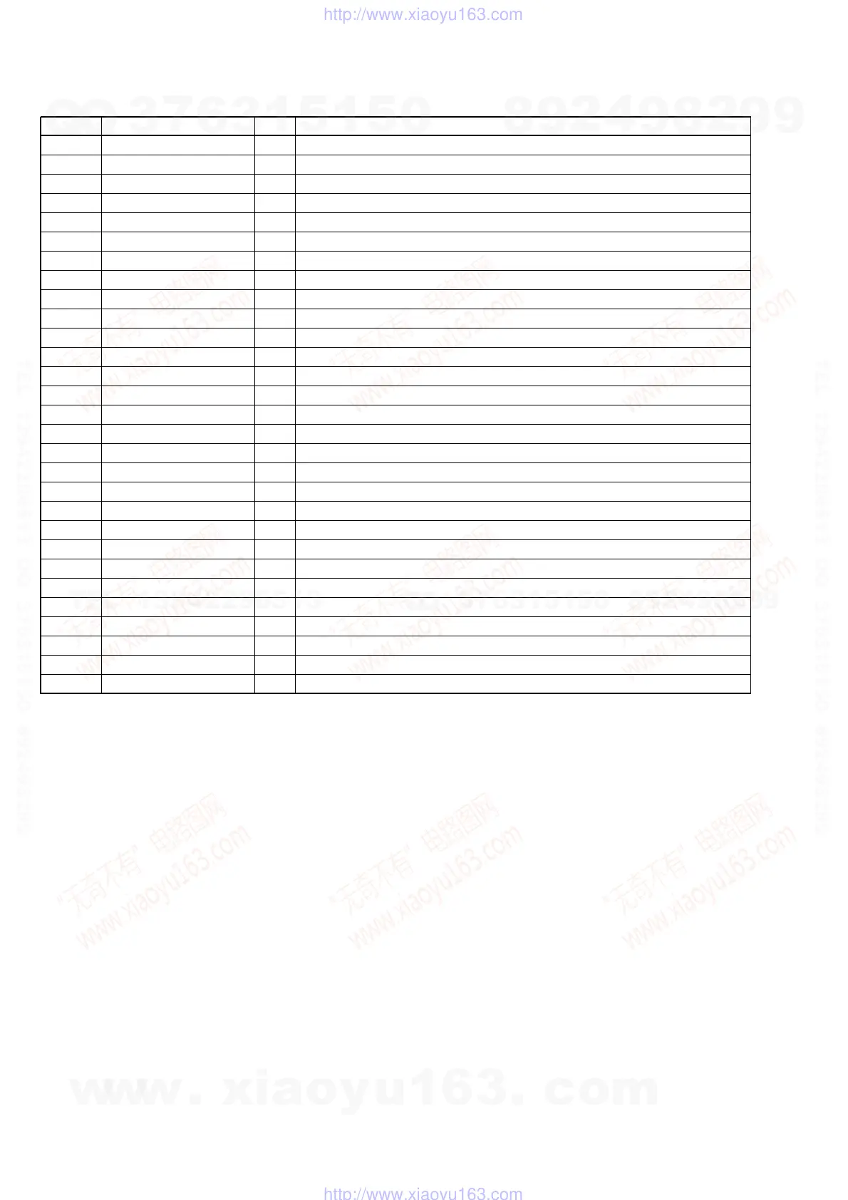
• IC101 µPD780232GC-504-8BT-A (SYSTEM CONTROL) (PANEL Board)
Pin No. Pin Name I/O Pin Description
1 VDD — Power supply pin (+3.3 V)
2 VSS — Ground pin
3X1ISystem clock signal input (5 MHz)
4X2ISystem clock signal input (5 MHz)
5ICIDirectly connect to ground.
6 RESET I Reset signal input (active L)
7 S-CLK I Serial clock signal input
8S-IN I Serial data in signal input
9 S-OUT O Serial data out signal output
10 to 14 NC-L O Not used in this set. (Fixed at L.)
15 VOL-A I VOLUME encoder in A signal input
16 VOL-B I VOLUME encoder in B signal input
17 NC-L I Not used in this set. (Fixed at L.)
18 AVSS — Analog ground pin
19 NC-L I Not used in this set. (Fixed at L.)
20 to 22 KEY3 to KEY1 I Key in signal input
23 VSS — Ground pin
24 AVDD — Analog power supply pin (+3.3 V)
25 VDD — Power supply pin (+3.3 V)
26 to 33 NC-L I Not used in this set. (Fixed at L.)
34 to 39 PS07 to PS12 O Illumination LED drive control signal output (L: OFF, H: ON)
40 MULTI/I-BASS O Not used in this set. (Fixed at L.)
41 NC O Not used. (Open)
42, 43 NC-L O Not used in this set. (Fixed at L.)
44 to 58 S1 to S15 O FL segment control signal output (L: OFF, H: ON)
59 VDD — Power supply pin (+3.3 V)
60 V.LOAD I V.LOAD signal input
61 to 66 S16 to S21 O FL segment control signal output (L: OFF, H: ON)
67 to 80 G1 to G13 O FL grid control signal output (L: OFF, H: ON)
w
w
w
.
x
i
a
o
y
u
1
6
3
.
c
o
m
Q
Q
3
7
6
3
1
5
1
5
0
9
9
2
8
9
4
2
9
8
T
E
L
1
3
9
4
2
2
9
6
5
1
3
9
9
2
8
9
4
2
9
8
0
5
1
5
1
3
6
7
3
Q
Q
TEL 13942296513 QQ 376315150 892498299
TEL 13942296513 QQ 376315150 892498299
http://www.xiaoyu163.com
http://www.xiaoyu163.com
 Loading...