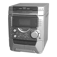
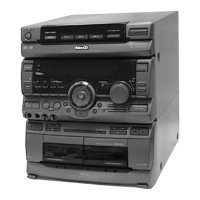
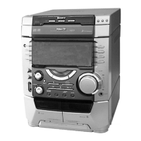
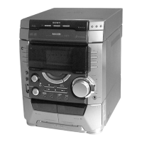
– 28 –
VIDEO BOARD IC701 HD6433032SK12F (CD MECHANISM CONTROLLER)
Pin No. Pin Name I/O Function
1 CMD0 I/O
2 CMD1 I/O
3 CMD2 I/O
4 CMD3 I/O
5 SACK O
Data acknowledge output to the IIC interface controller (IC901)
6 QINT I
Interrupt status input from the IIC interface controller (IC901)
7 VDAC-XLAT O
Serial data latch pulse output to the video D/A converter (IC401)
8 DF-XLAT O
Serial data latch pulse output to the D/A converter/digital filter (IC101)
9 P90/TXD O
Transmit data output terminal Not used (open)
10 SUBQ I
Sub-code Q data signal input from the CXD2545Q (IC101)
11 SQCK O
Sub-code Q data transfer clock signal output to the CXD2545Q (IC101)
12 VSS —
Ground terminal
13 D0 I/O
14 D1 I/O
15 D2 I/O
16 D3 I/O
17 D4 I/O
18 D5 I/O
19 D6 I/O
20 D7 I/O
21 VCC —
Power supply terminal (+5V)
22 A0 O
23 A1 O
24 A2 O
25 A3 O
26 A4 O
27 A5 O
28 A6 O
29 A7 O
30 VSS —
Ground terminal
31 A8 O
32 A9 O
33 A10 O
Address signal output to the S-RAM (IC751)
34 A11 O
35 A12 O
36 A13 O
37 A14 O
38 A15 O
39 A16 O
40 A17 O
41 A18 O
42 A19 O
Address signal output terminal Not used (open)
43 WAIT I
Wait signal input from the MPEG audio/video decoder (IC201)
44 MD0 I
Mode selection terminal (fixed at “H”)
45 MD1 I
Mode selection terminal (fixed at “L”)
46 Φ O
System clock signal output terminal Not used (open)
Two-way data bus with the IIC interface controller (IC901)
Two-way data bus with the S-RAM (IC751)
Address signal output to the S-RAM (IC751)
Address signal output terminal Not used (open)
Address signal output to the MPEG audio/video decoder (IC201) and S-RAM (IC751)
Address signal output terminal Used for chip enable signal output to the S-RAM (IC751)