EasyManua.ls Logo

Sony HCD-VX88 User Manual

Sony HCD-VX88
84 pages
To Next Page IconTo Next Page
Page #1 background imageLoading...
Page #1 background image
1
Amplifier section
The following measured at AC 120, 220, 240V
50/60 Hz
DIN power output (rated) 160 + 160 watts
(6 ohms at 1 kHz, DIN)
Continuous RMS power output (reference)
200 + 200 watts
(6 ohms at 1 kHz,
10% THD)
Inputs
MD/VIDEO (AUDIO) IN: voltage 450 mV/250 mV,
(phono jacks) impedance 47 kilohms
MIC: sensitivity 1 mV,
(phone jack) impedance 10 kilohms
Outputs
VIDEO OUT: max. output level 1 Vp-p,
(Phono jack) unbalanced, Sync
negative, load impedance
75 ohms
S-VIDEO OUT: Y: 1 Vp-p, unbalanced
(4 pin/mini-DIN jack) Sync negative
C: 0.286 Vp-p
load impedence 75 ohms
PHONES: accepts headphones of 8
(stereo mini jack) ohms or more
FRONT SPEAKER: accepts impedance of 6 to
16 ohms
SATELLITE SPEAKER: accepts impedance of 6 to
16 ohms
VIDEO CD/CD player section
System Compact disc and digital
audio system
Laser Semiconductor laser
(λ=780nm)
Emission duration:
continuous
Laser output Max. 44.6
µ
W*
*This output is the value
measured at a distance of
200 mm from the
objective lens surface on
the Optical Pick-up Block
with 7 mm aperture.
Frequency response 2 Hz – 20 kHz (±0.5 dB)
Wavelength 780 – 790 nm
Signal-to-noise ratio More than 90 dB
Dynamic range More than 90 dB
Video color system format
NTSC, PAL
CD OPTICAL DIGITAL OUT
(Square optical connector jack, rear panel)
Wavelength 660 nm
Output Level –18 dBm
Tape player section
Recording system 4-track 2-channel stereo
Frequency response 40 – 13,000 Hz (±3 dB),
(DOLBY NR OFF) using Sony TYPE I
cassette
40 – 14,000 Hz (±3 dB),
using Sony TYPE II
cassette
Tuner section
FM stereo, FM/AM superheterodyne tuner
FM tuner section
Tuning range 87.5 – 108.0 MHz
Antenna FM lead antenna
Antenna terminals 75 ohm unbalanced
Intermediate frequency 10.7 MHz
AM tuner section
Tuning range
Middle Eastern models: 531 – 1,602 kHz
(with the interval set at 9
kHz)
Other models: 531 – 1,602 kHz
(with the interval set at 9
kHz)
530 – 1,710 kHz
(with the interval set at 10
kHz)
Antenna AM loop antenna
Antenna terminals External antenna terminal
Intermediate frequency
450 kHz
HCD-VX88
SERVICE MANUAL
HCD-VX88 is the tuner, tape player, VIDEO CD/
CD player and amplifier section in MHC-VX88.
SPECIFICATIONS
COMPACT DISC DECK RECEIVER
E Model
This stereo system is equipped with the Dolby B-
type noise reduction system*.
* Manufactured under license from Dolby
Laboratories Licensing Corporation.
DOLBY and the double-D symbol ; are
trademarks of Dolby Laboratories Licensing
Corporation.
— Continued on next page —
Model Name Using Similar Mechanism HCD-VX77
CD
CD Mechanism Type CDM58-K2BD37A
Section
Base Unit Name BU-K2BD37A
Optical Pick-up Name KSM-213DAP/Z-NP
TAPE
Model Name Using Similar Mechanism HCD-VX77
Section
Tape Transport Mechanism Type TCM-230AWR11
9-929-218-14 Sony Corporation
2002K0500-1 Home Audio Company
C 2002.11 Published by Sony Engineering Corporation
Ver 1.3 2002.11
Question and Answer IconNeed help?

Do you have a question about the Sony HCD-VX88 and is the answer not in the manual?

Sony HCD-VX88 Specifications

General IconGeneral
BrandSony
ModelHCD-VX88
CategoryStereo System
LanguageEnglish

Summary

General

SECTION 1 SERVICE NOTES

SELF-DIAGNOSIS

System diagnosis function for VIDEO and AUDIO decoder sections.

SECTION 2 GENERAL

LOCATION OF CONTROLS

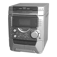
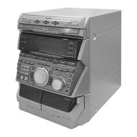
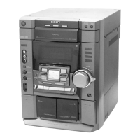
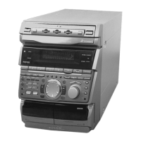
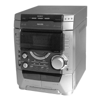
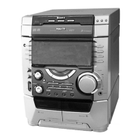
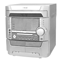
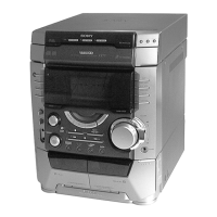
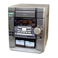
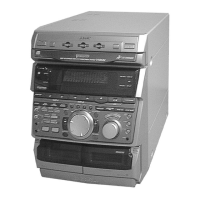
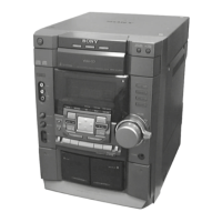
Identifies the location and function of all front panel controls and indicators.

SECTION 3 DISASSEMBLY

COVER (TOP)

Procedure for removing the top cover of the unit.

LOADING PANEL ASS'Y

Steps for removing the loading panel assembly.

SECTION 4 TEST MODE

[MC Cold Reset]

Resets the system to initial conditions, clearing all preset data.

[CD Ship Mode]

Moves pickup to a stable position for shipping or transport.

[GC Test Mode]

Checks software version, FL tube, LED, keyboard, and VACS status.

SECTION 5 AGING MODE

Error display

Indicates errors encountered during aging mode operation and displays the error status.

VIDEO CD COLOR-BARS MODE

SECTION 5 MECHANICAL ADJUSTMENTS

Precautions

General safety and handling guidelines for mechanical adjustments.

SECTION 6 ELECTRICAL ADJUSTMENTS

Record/Playback Head Azimuth Adjustment

Procedure for aligning the record/playback head azimuth for optimal performance.

SECTION 7 DIAGRAMS

7-1. CIRCUIT BOARDS LOCATION

Diagram showing the physical layout of all circuit boards within the system.

7-2. BLOCK DIAGRAMS

-TUNER/CD SECTION –

Block diagram illustrating the signal flow for the tuner and CD sections.

VIDEO SECTION

Block diagram illustrating the signal flow for the video processing section.

7-3. PRINTED WIRING BOARD - BD SECTION -

【BD BOARD】 (SIDE A)

Component layout for the BD board, viewed from the component side.

【BD BOARD】(SIDE B)

Component layout for the BD board, viewed from the solder side.

7-4. SCHEMATIC DIAGRAM - BD SECTION -

【BD BOARD】

Schematic diagram detailing the electronic connections of the BD board.

7-5. PRINTED WIRING BOARD - VIDEO SECTION -

【VIDEO BOARD】 (SIDE A)

Component layout for the video board, viewed from the component side.

【VIDEO BOARD】 (SIDE B)

Component layout for the video board, viewed from the solder side.

7-6. SCHEMATIC DIAGRAM - VIDEO (1/3) SECTION –

VIDEO BOARD (1/3)

Schematic diagram for the first part of the video section.

7-7. SCHEMATIC DIAGRAM - VIDEO (2/3) SECTION –

VIDEO BOARD (2/3)

Schematic diagram for the second part of the video section.

7-8. SCHEMATIC DIAGRAM - VIDEO (3/3) SECTION –

VIDEO BOARD (3/3)

Schematic diagram for the third part of the video section.

7-9. PRINTED WIRING BOARD - MAIN SECTION -

【MAIN BOARD】

Component layout for the main board.

7-10. SCHEMATIC DIAGRAM - MAIN (1/3) SECTION –

【MAIN BOARD】 (1/3)

Schematic diagram for the first part of the main board.

7-11. SCHEMATIC DIAGRAM - MAIN (2/3) SECTION –

【MAIN BOARD】(2/3)

Schematic diagram for the second part of the main board.

7-12. SCHEMATIC DIAGRAM - MAIN (3/3) SECTION –

【MAIN BOARD】 (3/3)

Schematic diagram for the third part of the main board.

7-13. PRINTED WIRING BOARD - POWER AMP SECTION -

【POWER AMP BOARD】

Component layout for the power amplifier board.

7-14. SCHEMATIC DIAGRAM - POWER AMP SECTION -

【POWER AMP BOARD】

Schematic diagram for the power amplifier section.

7-15. PRINTED WIRING BOARDS - PANEL SECTION -

【CD SWITCH BOARD】

Component layout for the CD switch board.

【PANEL BOARD】

Component layout for the main panel board.

7-16. SCHEMATIC DIAGRAM - PANEL SECTION -

【PANEL BOARD】

Schematic diagram for the panel section.

7-17. PRINTED WIRING BOARDS - LEAF SW SECTION -

【LEAF SW BOARD】

Component layout for the leaf switch board.

【HEAD (A) BOARD】

Component layout for the head (A) board.

【HEAD (B) BOARD】

Component layout for the head (B) board.

7-18. SCHEMATIC DIAGRAM - LEAF SW SECTION -

【LEAF SW BOARD】

Schematic diagram for the leaf switch section.

7-19. PRINTED WIRING BOARDS - DRIVER SECTION -

【MOTOR BOARD】

Component layout for the motor driver board.

【SENSOR BOARD】

Component layout for the sensor board.

【DRIVER BOARD】

Component layout for the driver board.

7-20. SCHEMATIC DIAGRAM - DRIVER SECTION –

【MOTOR BOARD】

Schematic diagram for the motor driver section.

【SENSOR BOARD】

Schematic diagram for the sensor section.

【DRIVER BOARD】

Schematic diagram for the driver section.

7-21. PRINTED WIRING BOARD - TRANS SECTION –

【TRANS BOARD】

Component layout for the transformer board.

7-22. SCHEMATIC DIAGRAM - TRANS SECTION –

【TRANS BOARD】

Schematic diagram for the transformer section.

7-23. IC PIN FUNCTION DESCRIPTION

• IC101 DIGITAL SERVO...

Detailed pin functions for the digital servo processor and D/A converter IC.

7-24. IC BLOCK DIAGRAMS

• BD Board -

Block diagrams illustrating the internal circuitry of the BD board ICs.

SECTION 8 EXPLODED VIEWS

(1) COVER SECTION

Exploded view showing the parts and assembly of the unit's cover section.

(2) FRONT PANEL SECTION

Exploded view showing the parts and assembly of the front panel section.

(3) CHASSIS SECTION

Exploded view showing the parts and assembly of the chassis section.

(4) TAPE MECHANISM DESK SECTION (TCM-230AWR11)

Exploded view showing the parts and assembly of the tape mechanism deck.

(5) CD MECHANISM DECK SECTION (CDM58-K2BD37A)

Exploded view showing the parts and assembly of the CD mechanism deck.

(6) BASE UNIT SECTION (BU-K2BD37A)

Exploded view showing the parts and assembly of the base unit section.

SECTION 9 ELECTRICAL PARTS LIST

< CAPACITOR >

List of capacitors used in the electrical parts list.

< IC >

List of integrated circuits used in the electrical parts list.

< TRANSISTOR >

List of transistors used in the electrical parts list.

REVISION HISTORY

Related product manuals